Thin film transistor array substrate, manufacturing method thereof and touch display panel

a technology of thin film transistor array and manufacturing method, which is applied in the field of touch technology and display technology, can solve the problems of reducing the real thickness of the liquid crystal display panel, affecting the final display effect, and affecting the display effect, so as to reduce the thickness and improve the display effect.

Inactive Publication Date: 2017-08-17
WUHAN CHINA STAR OPTOELECTRONICS TECH CO LTD
View PDF7 Cites 8 Cited by
  • Summary
  • Abstract
  • Description
  • Claims
  • Application Information

AI Technical Summary

Benefits of technology

[0025]In the present invention, the planarization layer on the thin film transistor array substrate is optimally designed. The grooves are disposed on the planarization layer to receive the touch control electrode lead wires, so that the touch control electrode lead wires do not protrude from the planarization layer but in the same plane with the planarization layer, thereby making the upper surface of the film layer formed above the touch control electrode lead wires to be also a planar. In such a structure, even if a poor accuracy of combining the color filter substrate and the thin film transistor array substrate causes that the photo spacers cannot correspond to the locations of the touch control electrode lead wires accurat...

Problems solved by technology

If the color filter substrate cannot match with the thin film transistor array substrate accurately, the photo spacer will slip off from the lead wires, thereby affecting the real thickness of a liquid crystal display to cause the bad display effect.
Although the cylindrical spacers can still...

Method used


Image

  • Thin film transistor array substrate, manufacturing method thereof and touch display panel
  • Thin film transistor array substrate, manufacturing method thereof and touch display panel
  • Thin film transistor array substrate, manufacturing method thereof and touch display panel

Examples


Embodiment Construction

[0036]The following content combines with the figures and the embodiments for describing the present invention in detail. It is obvious that the following embodiments are only some embodiments of the present invention. For an ordinary person skilled in the art without any creative effort, other embodiments obtained thereby are still covered by the present invention.

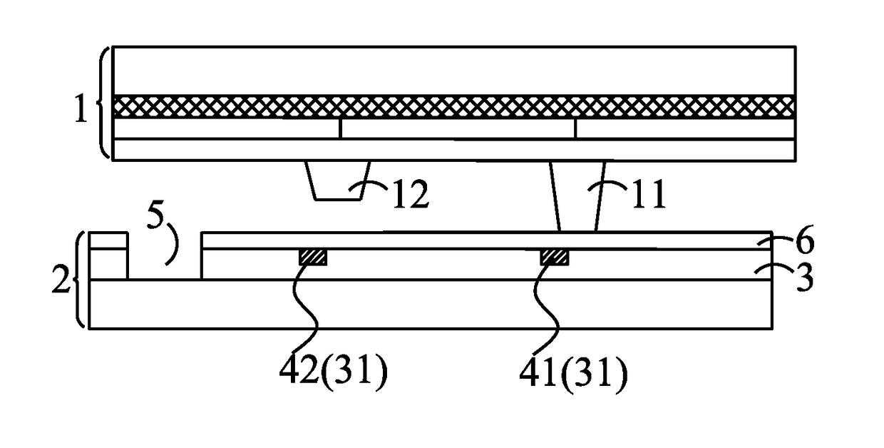
[0037]Referring to FIG. 6, a touch control display panel in accordance with an embodiment includes a color filter (CF) substrate 1, a thin film transistor (TFT) array substrate 2, and a liquid crystal layer (not shown) placed between the color filter substrate 1 and the thin film transistor array substrate 2.

[0038]A first cylindrical spacer 11 and a second cylindrical spacer 12 are disposed on the color filter substrate 1, and extend in a direction from a lower surface of the color filter substrate 1 toward the thin film transistor array substrate 2. A height of the first cylindrical spacer 11 is higher than a height of t...


PUM


Abstract

The invention provides a thin film transistor array substrate, a manufacturing method thereof, and a touch control display panel. The touch control display panel includes a color filter substrate, a thin film transistor array substrate mentioned above, and a liquid crystal layer and photo spacers located between the two substrates. When the color filter substrate combined with the thin film transistor array substrate face to face, the photo spacers is located therebetween. The thin film transistor array substrate has a planarization layer therein. The planarization layer is recessed to a plurality of grooves arranged at intervals. A plurality of touch control electrode lead wires are received in the plurality of grooves. Upper surfaces of the plurality of touch control electrode lead wires and an upper surface of the planarization layer are in a same plane.

Description

BACKGROUND OF THE INVENTION[0001]1. Field of the Invention[0002]The present invention relates to touch technology and display technology fields, especially relates to a thin film transistor array substrate, a manufacturing method thereof, and a touch display panel having the thin film transistor array substrate.[0003]2. Description of Related Art[0004]With the development of touch technology and display technology, touch display panels have been widely used in smart phones, tablet computers, and other intelligent electronic products, which brings more convenient experience for human computer interaction.[0005]At present, according to their composition structures, touch display panels can be divided into add on mode touch panels, on-cell touch panels, in-cell touch panels, etc., wherein the touch control electrode of the in-cell touch panel is embedded into the inner side of a touch panel, which can effectively reduce the thickness of the whole module to make it much thinner and more...

Claims


Application Information

Patent Timeline
IPC IPC(8): G06F3/041G02F1/1333G02F1/1339G02F1/1368G02F1/1362G06F3/047G02F1/1335H01L21/77
CPCG06F3/0412G06F3/0416G06F3/047G02F1/13338G02F1/133514G02F2001/136295G02F1/136286G02F1/13394G06F2203/04103G02F2001/133357G02F2001/13398G02F1/1368H01L21/77H01L27/02G02F1/133357G02F1/13398
Inventor GONG, QIANG
Owner WUHAN CHINA STAR OPTOELECTRONICS TECH CO LTD
Why Eureka
Try Eureka