Manufacturing method of organic light emitting device, organic light emitting device and electronic apparatus

a technology which is applied in the field of manufacturing methods of organic light and organic light emitting devices, organic light and electronic devices, can solve the problems of weak adhesion of color filters that correspond to predetermined subpixels, the area of pixels is becoming increasingly small, and the adhesion of color filters becomes even weaker. , to achieve the effect of enhancing the adhesion of the second color filter, and improving the wettability

Active Publication Date: 2017-08-17
SEIKO EPSON CORP
View PDF10 Cites 6 Cited by
  • Summary
  • Abstract
  • Description
  • Claims
  • Application Information

AI Technical Summary

Benefits of technology

[0019]By forming the color filter layer at a low temperature of less than or equal to 110° C., it is possible to suppress thermal degradation of the organic light emitting device.Application Example 5
[0024]By providing the second color filter so as to cover an end part of the first color filter, or in other words, by forming the second color filter to have a portion that overlaps with the first color filter in a planar fashion, it is possible to make the area of a portion in which the second color filter comes into contact with components other than the sealing layer larger than a case in which the second color filter does not overlap with the first color filter in a planar fashion, and therefore, to enhance the adhesion of the second color filter.
[0025]Furthermore, the second color filter includes a portion that comes into contact with a material of the same kind (the first color filter) in addition to a portion that comes into contact with a material of a different kind (the sealing layer). In the portion that comes into contact with a material of the same kind, the wettability and affinity (ease of attachment) of the second color filter are improved, and therefore, it is possible to enhance the adhesion of the second color filter.
[0028]By providing the second color filter so as to cover an end part of the third color filter, or in other words, by forming the second color filter to have a portion that overlaps with the third color filter in a planar fashion, it is possible to make the area of a portion in which the second color filter comes into contact with components other than the sealing layer larger than a case in which the second color filter does not overlap with the third color filter in a planar fashion, and therefore, to enhance the adhesion of the second color filter.
[0029]Furthermore, the second color filter includes a portion that comes into contact with a material of the same kind (the third color filter) in addition to a portion that comes into contact with a material of a different kind (the sealing layer). In the portion that comes into contact with a material of the same kind, the wettability and affinity (ease of attachment) of the second color filter are improved, and therefore, it is possible to enhance the adhesion of the second color filter.

Problems solved by technology

Furthermore, miniaturization and increases in the density of pixels are progressing in the display units of head-mounted displays and electronic viewfinders, and therefore, the area of the pixels is becoming increasingly small.
If the color filter layer is formed at a low temperature in order to suppress deterioration of the light emitting layer, adhesion of the color filter layer becomes weak in comparison with cases in which the color filter layer is formed at high temperature.
Furthermore, since the areas of the color filters that correspond to predetermined subpixels are smaller than the areas of other color filters, the adhesion of the color filters that correspond to predetermined subpixels becomes even weaker.
Therefore, there is a problem in that the adhesion of color filters that correspond to predetermined subpixels is weak, and likely to peel away in comparison with the color filters that correspond to other subpixels.

Method used


Image

  • Manufacturing method of organic light emitting device, organic light emitting device and electronic apparatus
  • Manufacturing method of organic light emitting device, organic light emitting device and electronic apparatus
  • Manufacturing method of organic light emitting device, organic light emitting device and electronic apparatus

Examples


embodiment 1

Summary of Organic EL Device

[0053]An organic EL device 100 according to Embodiment 1 is an example of “an organic light emitting device” in the present invention, and is a self-light emitting microdisplay that is suitable for use in a display unit of a head-mounted display that will be described later.

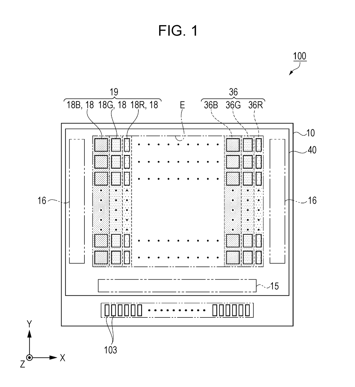
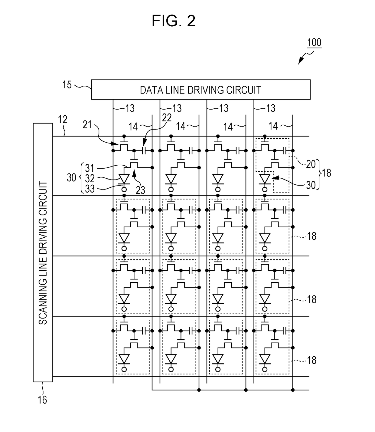
[0054]FIG. 1 is a schematic plan view that shows a summary of an organic EL device according to the present embodiment. FIG. 2 is an equivalent circuit diagram that shows an electrical configuration of the organic EL device according to the present embodiment.

[0055]Firstly, a summary of the organic EL device 100 according to the present embodiment will be described with reference to FIG. 1 and FIG. 2.

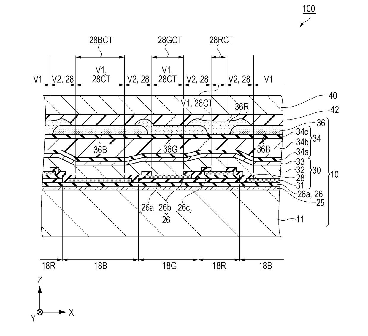
[0056]As shown in FIG. 1, the organic EL device 100 according to the present embodiment includes an element substrate 10 and a protective substrate 40. Both substrates are bonded to each other using a resin layer 42 (refer to FIG. 4) that will be described later.

[0057]The element substrate...

embodiment 2

[0135]FIG. 7 is a drawing that corresponds to FIG. 4, and is a schematic cross-sectional view that shows a summary of an organic EL device according to Embodiment 2. FIG. 8 is a process flow that shows a manufacturing method of a color filter layer. FIGS. 9A, 9B, 9C and 9D are drawings that correspond to FIG. 7, and are schematic cross-sectional views that show states after passing each process of the process flow that is shown in FIG. 8.

[0136]In an organic EL device 200 of the present embodiment, convex units 37 are provided between the second sealing layer 34c and the color filter layer 36. This feature is the main point of difference between the organic EL device 200 of the present embodiment and the organic EL device 100 of Embodiment 1.

[0137]Hereinafter, a summary of the organic EL device 200 according to the present embodiment will be described focusing on the points of difference with Embodiment 1 with reference to FIGS. 7 to 9D. Additionally, constituent elements that are th...

embodiment 3

Electronic Apparatus

[0159]FIG. 10 is a schematic view of a head-mounted display as an example of an electronic apparatus.

[0160]As shown in FIG. 10, a head-mounted display 1000 includes two display units 1001 which are provided to correspond to the left and right eyes. By mounting the head-mounted display 1000 on a head part in a manner similar to glasses, it is possible for an observer M to view characters, images and the like which are displayed on the display units 1001. For example, if an image in which a parallax in the left and right display units 1001 is taken into account is displayed, it is possible for the observer M to enjoy a stereoscopic image.

[0161]The display units 1001 are equipped with either the organic EL device 100 or the organic EL device 200 according to the abovementioned embodiments. In the abovementioned embodiments, a defect of the red coloring layers 36R, the bonding strength of which is weakest, peeling away is suppressed, and it is possible to stably manu...


PUM


Abstract

A manufacturing method of an organic light emitting device including a light emitting element that includes an organic light emitting layer, a sealing layer above the light emitting element, and a color filter layer above the sealing layer. The color filter layer includes a first color filter that transmits light of a first wavelength region and a second color filter that transmits light of a second wavelength region, an area of the second color filter is smaller than an area of the first color filter, and the method includes forming the first color filter, and forming the second color filter thereafter.

Description

BACKGROUND[0001]1. Technical Field[0002]The present invention relates to a manufacturing method of an organic light emitting device, an organic light emitting device that is manufactured by the manufacturing method, and an electronic apparatus in which the organic light emitting device is equipped.[0003]2. Related Art[0004]In comparison with non-light emitting type display apparatuses such as liquid crystal apparatuses, organic electroluminescence (hereinafter, referred to as EL) devices have an advantage from a point of thinning and weight reduction since backlighting is not required as a light source, and therefore, application in the display units of microdisplays such as head-mounted displays and electronic viewfinders is anticipated. Furthermore, miniaturization and increases in the density of pixels are progressing in the display units of head-mounted displays and electronic viewfinders, and therefore, the area of the pixels is becoming increasingly small.[0005]For example, JP...

Claims


Application Information

Patent Timeline
Patent Type & Authority Applications(United States)
IPC IPC(8): H01L27/32H01L51/52
CPCH01L27/322H01L27/3216H01L51/5265H10K71/00H10K50/84H10K59/876G02B5/201H10K59/352H10K59/38H10K50/00H10K50/80H10K50/852
Inventor AKAGAWA, SUGURUHANAMURA, YUKI
Owner SEIKO EPSON CORP
Why Eureka
Try Eureka