

Semiconductor device and method for manufacturing the same
- Summary
- Abstract
- Description
- Claims
- Application Information
AI Technical Summary
Benefits of technology
Problems solved by technology
Method used
Image

Examples
Embodiment Construction
[0055]Preferred embodiments of the present invention shall now be described in detail with reference to the attached drawings.
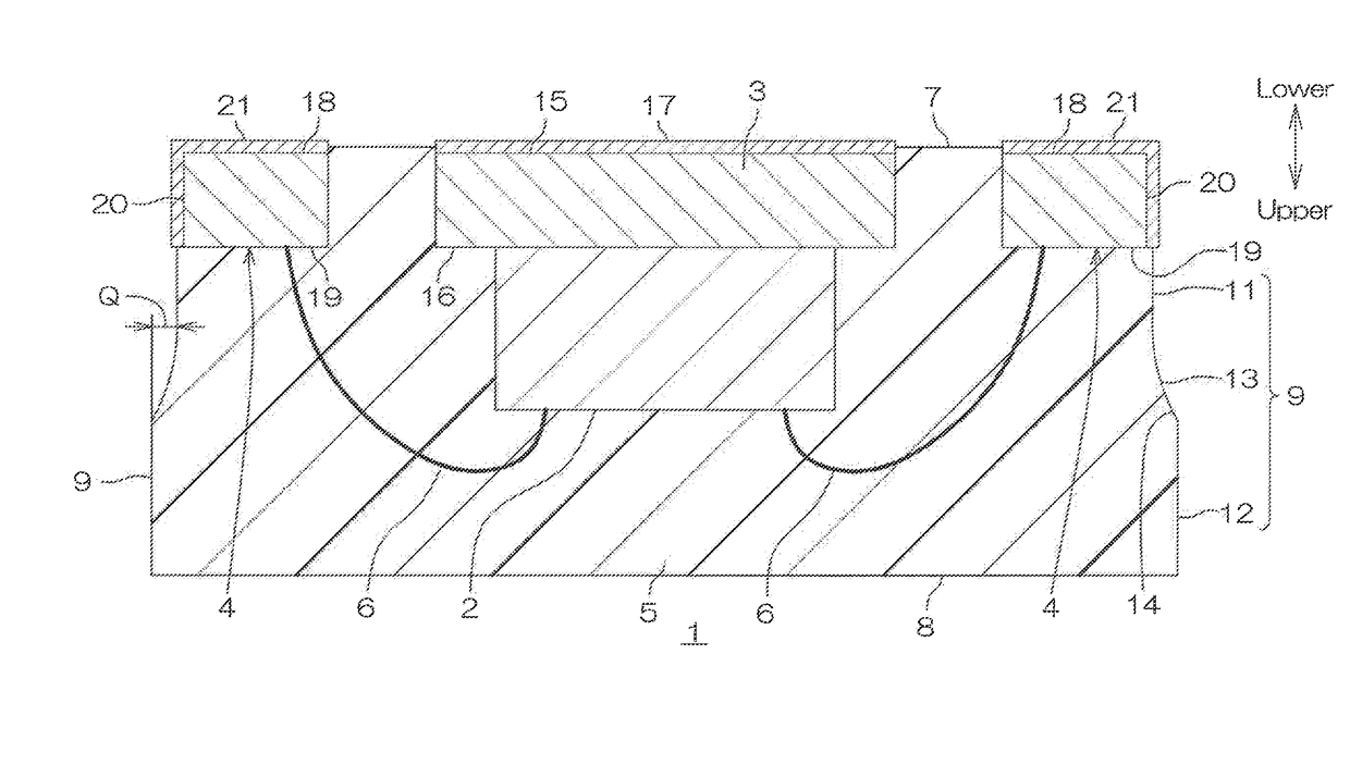
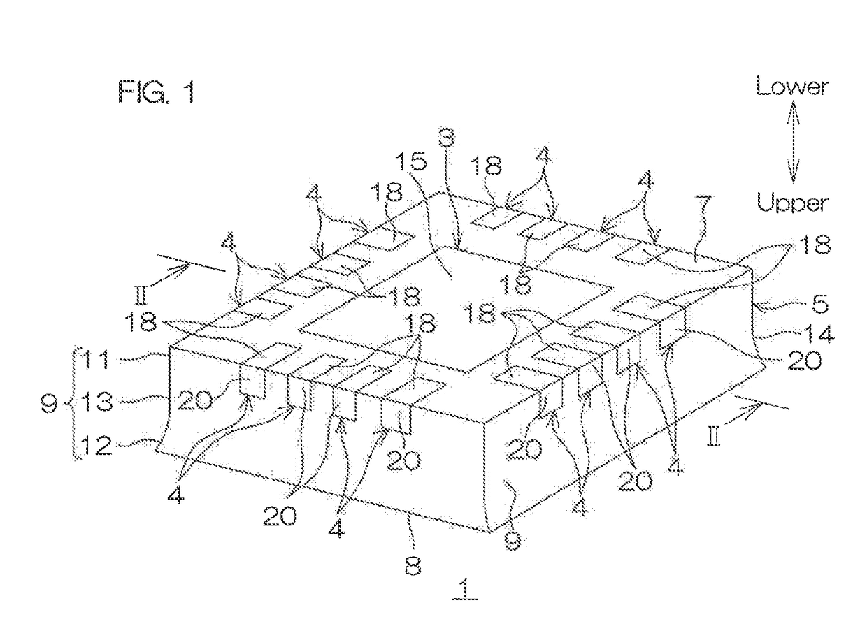
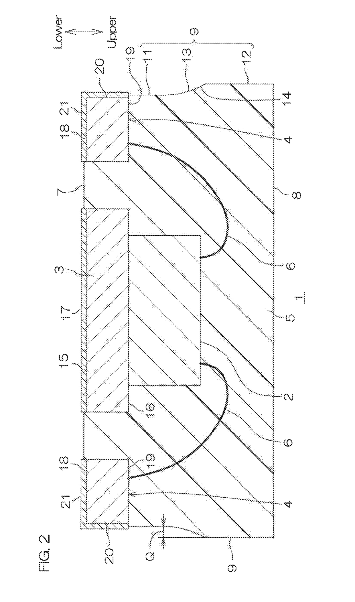
[0056]FIG. 1 is an illustrative perspective view of a semiconductor device according to a first preferred embodiment of the present invention as viewed from obliquely above. Also, FIG. 2 is an illustrative sectional view taken along line II-II in FIG. 1. FIG. 3 is an enlarged view of a portion including a lead at one side and a portion of a die pad of FIG. 2.
[0057]The semiconductor device 1 is a semiconductor device applying a QFN. The semiconductor device 1 includes a semiconductor chip 2, a die pad 3, a plurality of leads 4, and a sealing resin 5. The die pad 3 is arranged to support the semiconductor chip 2. The plurality of leads 4 are electrically connected to the semiconductor chip 2. The sealing resin 5 seals the semiconductor chip 2, the die pad 3, and the plurality of leads 4.
[0058]The semiconductor chip 2 is die bonded onto the die pad 3 in a state ...
PUM
 Abstract
Description
Claims
Application Information