Manufacturing method of circuit board

Active Publication Date: 2017-09-21
UNIMICRON TECH CORP
View PDF2 Cites 0 Cited by
  • Summary
  • Abstract
  • Description
  • Claims
  • Application Information

AI Technical Summary

Benefits of technology

[0018]Based on the above, in the invention, a patterned photoresist layer is firmly formed on a film layer below via an adhesive layer, and therefore the patterned photoresist layer can be effectively prevented f

Problems solved by technology

However, after NIL transfers a pattern to a photoresist material, comprehensive exposure needs to be performed, and therefore the patterned photoresist layer to be formed and unnecessary residual photoresist material are both exposed to light.
As a result, the residual photoresist layer cannot be removed by a developing solution in a simple manner.
Therefore, unnecessary residual photoresist material needs to be removed using inductively-coupled plasma (ICP) or reactive ion etching (RIE)

Method used


Image

  • Manufacturing method of circuit board
  • Manufacturing method of circuit board
  • Manufacturing method of circuit board

Examples


first embodiment

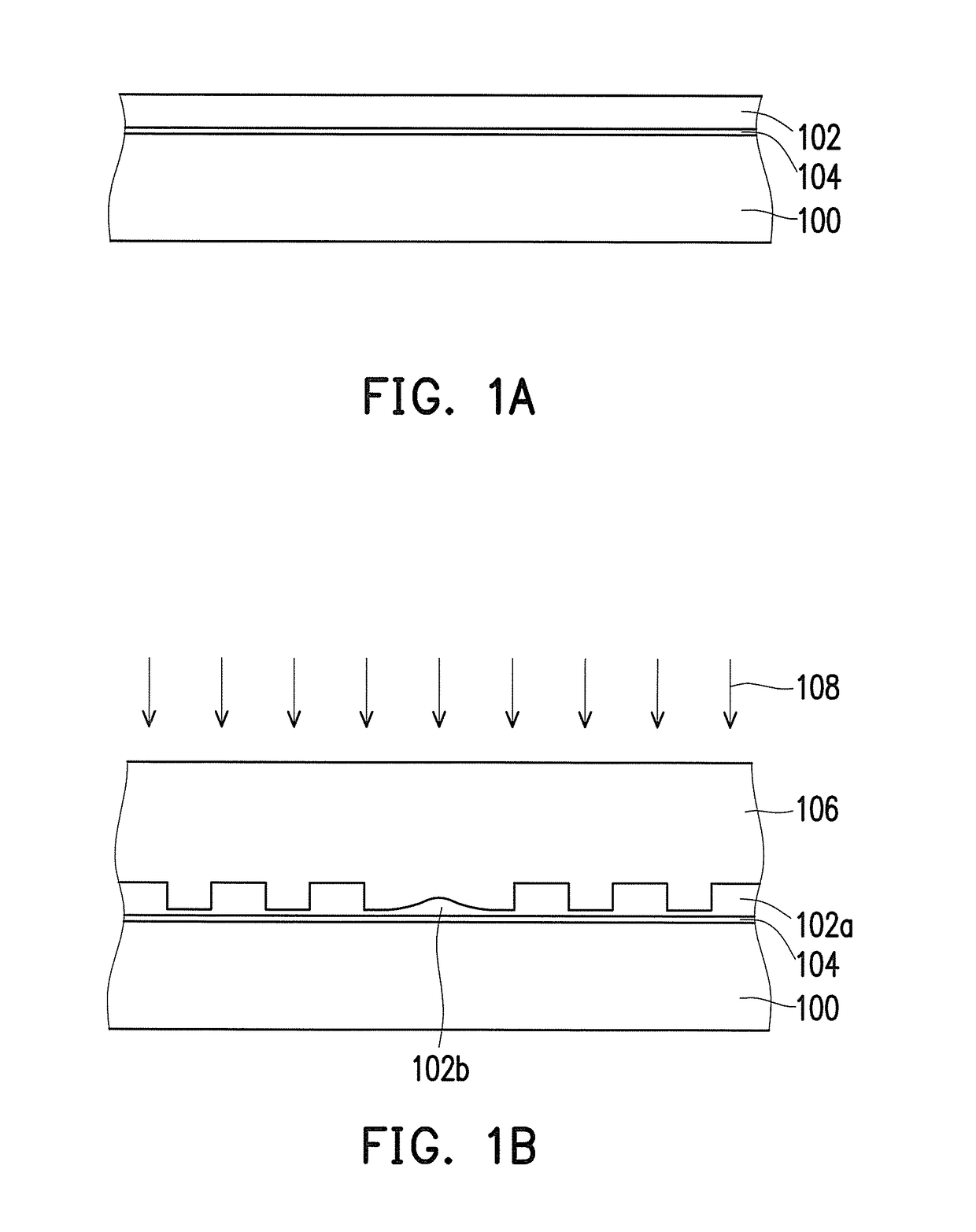
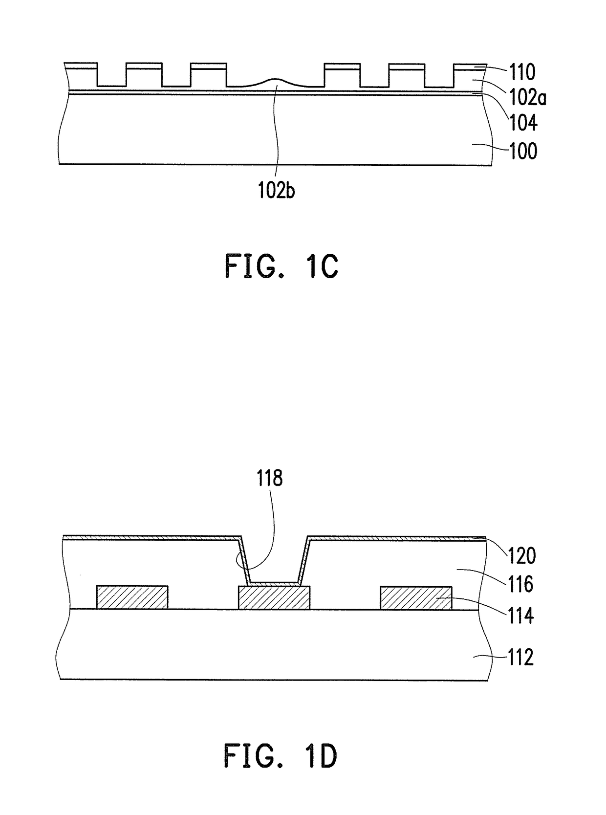
[0024]FIG. 1A to FIG. 1G are cross-sectional schematics of the manufacturing process of a circuit board shown according to the first embodiment of the invention. First, referring to FIG. 1A, a photoresist material layer 102 is formed on a carrier substrate 100. The carrier substrate 100 is, for instance, a glass substrate, a copper clad laminate, a Si laminate, or a ceramic laminate. In the present embodiment, the photoresist material layer 102 is a photoresist material layer curied after UV irradiation, but the invention is not limited thereto. Moreover, in the present embodiment, a release layer 104 can further be formed between the carrier substrate 100 and the photoresist material layer 102. The release layer 104 can facilitate the separation of a patterned photoresist layer formed by the photoresist material layer 102 and the carrier substrate 100 in a subsequent process.

[0025]Next, referring to FIG. 1B, an imprinting process is performed on the photoresist material layer 102 v...

second embodiment

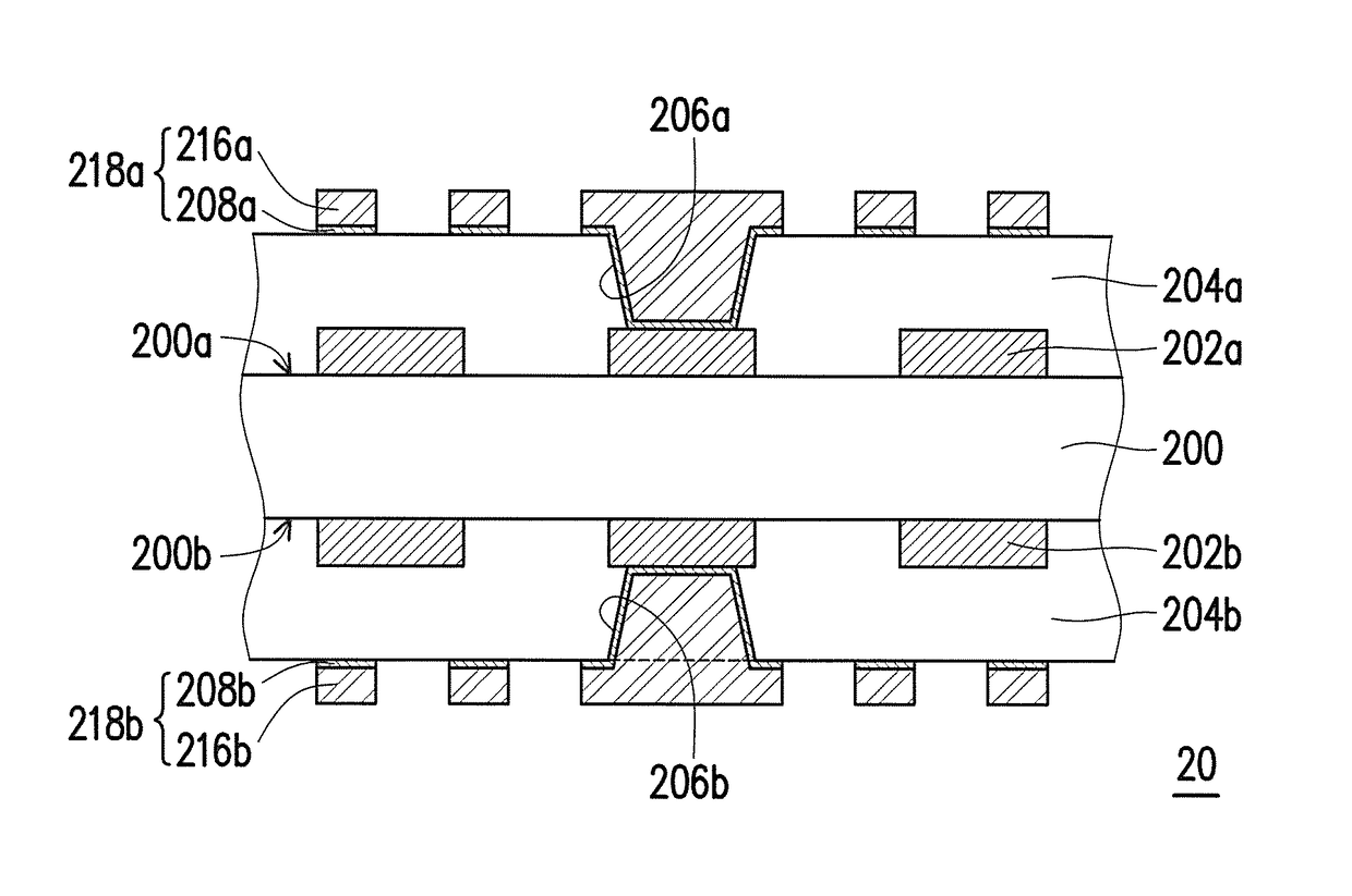
[0032]FIG. 2A to FIG. 2E are cross-sectional schematics of the manufacturing process of a circuit board shown according to the second embodiment of the invention. First, referring to FIG. 2A, a circuit pattern 202a is formed on a first surface 200a of a dielectric substrate 200, and a circuit pattern 202b is formed on a second surface 200b of the dielectric substrate 200. The material of the dielectric substrate 200 is, for instance, epoxy resin, glass fiber cloth, or ceramic. The material of the circuit patterns 202a and 202b is, for instance, copper. Then, a dielectric layer 204a is formed on the first surface 200a and a dielectric layer 204b is Ruined on the second surface 200b. The dielectric layer 204a covers the circuit pattern 202a on the first surface 200a and the dielectric layer 204b covers the circuit pattern 202b on the second surface 200b. The material of the dielectric layers 204a and 204b is, for instance, epoxy resin. The dielectric layers 204a and 204b are, for inst...


PUM

PropertyMeasurementUnit
Electrical conductoraaaaaaaaaa
Sensitivityaaaaaaaaaa
Mechanical forceaaaaaaaaaa

Abstract

A manufacturing method of a circuit board including the following steps is provided. A carrier substrate is provided. A patterned photoresist layer is formed on the carrier substrate. An adhesive layer is formed on the top surface of the patterned photoresist layer. A dielectric substrate is provided. A circuit pattern and a dielectric layer covering the circuit pattern are formed on the dielectric substrate, wherein the dielectric layer has an opening exposing a portion of the circuit pattern. The adhesive layer is adhered to the dielectric layer in a direction that the adhesive layer faces of the dielectric layer. The carrier substrate is removed. A patterned metal layer is formed on a region exposed by the patterned photoresist layer. The patterned photoresist layer is removed. The adhesive layer is removed.

Description

CROSS-REFERENCE TO RELATED APPLICATION[0001]This application claims the priority benefit of U.S. provisional application Ser. No. 62 / 309,930, filed on Mar. 17, 2016. The entirety of the above-mentioned patent application is hereby incorporated by reference herein and made a part of this specification.BACKGROUND OF THE INVENTION[0002]Field of the Invention[0003]The invention relates to a manufacturing method of a circuit board, and more particularly, to a manufacturing method of a circuit board fixing a patterned photoresist layer using an adhesive layer.[0004]Description of Related Art[0005]Nano-imprint lithography (NIL) is a technique for manufacturing fine circuits and is extensively applied in the LED and OLED industries. NIL includes pressing a mold prototype having a pattern (generally referred to as mold, stamp, or template) on a photoresist material to mechanically deform the mold prototype so as to precisely transfer a fine pattern. Therefore, once the manufacture of the mol...

Claims


Application Information

Patent Timeline
IPC IPC(8): H05K3/00H05K3/10H05K3/46
CPCH05K3/0023H05K3/4644H05K2203/0562H05K2203/0108H05K2203/0369H05K3/108G03F7/0002H05K3/465Y10T29/49124Y10T29/49155Y10T29/5313G03F7/162G03F7/20H05K1/115H05K3/06H05K3/064H05K2201/091H05K2203/0548H05K2203/0502
Inventor CHENG, SHIH-LIAN
Owner UNIMICRON TECH CORP
Why Eureka
Try Eureka