Methods and apparatus for polarized wafer inspection

a technology of polarized wafers and inspection methods, applied in semiconductor/solid-state device testing/measurement, instruments, material analysis, etc., can solve the problems of increasing the defect signal to noise ratio of fabricated devices, increasing the risk of failure, so as to achieve the effect of maximizing the defect signal to noise ratio

Active Publication Date: 2017-09-28
KLA CORP
View PDF0 Cites 27 Cited by
  • Summary
  • Abstract
  • Description
  • Claims
  • Application Information

AI Technical Summary

Benefits of technology

[0006]In one embodiment, an inspection system for inspecting a semiconductor sample is disclosed. This system comprises an illumination optics subsystem for generating and directing an incident beam towards a defect on the surface of a wafer. The illumination optics subsystem includes a light source for generating the incident beam and one or more polarization components for adjusting a ratio and / or phase difference between the two base vectors for the incident beam's electric field components. The system further includes a collection optics subsystem for collecting scattered light from the defect and / or surface in response to the incident beam, and the collection optics subsystem comprises an adjustable aperture at the pupil plane, followed by a rotatable waveplate for adjusting the phase difference for the collected scattered light's electric field components, followed by a rotatable analyzer. The system also includes a controller that is configured for (i) selecting a polarization of the incident beam, (ii) obtaining a defect scattering map, (iii) obtaining a surface scattering map, and (iv) determining a configuration of the one or more polarization components, aperture mask, and rotatable waveplate, and analyzer based on analysis of the defect and scattering map so as to maximize a defect signal to noise ratio.
[0011]In another embodiment, the invention pertains to a method of inspecting a semiconductor sample. The method includes (i) in an illumination optics subsystem of an inspection system, generating and directing an incident beam at a selected polarization state towards a defect on a surface of a wafer, wherein the illumination optics subsystem of the inspection system includes a light source for generating the incident beam and one or more polarization components for adjusting a ratio and / or phase difference for the incident beam's electric field components, (ii) in a collection optics subsystem of an inspection system, collecting scattered light from the defect and / or surface in response to the incident beam, wherein the collection optics subsystem of the inspection system comprises an adjustable aperture at the pupil plane, followed by a rotatable waveplate for adjusting a phase difference of electric field components of the collected scattered light, followed by a rotatable analyzer, (iii) obtaining a defect scattering map based on the collected scattered light, (iv) obtaining a surface scattering map based on the collected scattered light, and (v) determining a configuration of the one or more polarization components, aperture mask, and rotatable waveplate, and analyzer based on analysis of the defect and surface scattering map so as to maximize a defect signal to noise ratio.

Problems solved by technology

Generally, the industry of semiconductor manufacturing involves highly complex techniques for fabricating integrating circuits using semiconductor materials which are layered and patterned onto a substrate, such as silicon.
Due to the large scale of circuit integration and the decreasing size of semiconductor devices, the fabricated devices have become increasingly sensitive to defects.
That is, defects which cause faults in the device are becoming increasingly smaller.

Method used


Image

  • Methods and apparatus for polarized wafer inspection
  • Methods and apparatus for polarized wafer inspection
  • Methods and apparatus for polarized wafer inspection

Examples


Embodiment Construction

[0036]In the following description, numerous specific details are set forth in order to provide a thorough understanding of the present invention. The present invention may be practiced without some or all of these specific details. In other instances, well known component or process operations have not been described in detail to not unnecessarily obscure the present invention. While the invention will be described in conjunction with these specific embodiments, it will be understood that it is not intended to limit the invention to these embodiments.

[0037]Certain inspection system embodiments are described herein as being configured for inspecting semiconductor structures. Other types of structures, such as solar panel structures, optical disks, etc., may also be inspected or imaged using the inspection apparatus of the present invention.

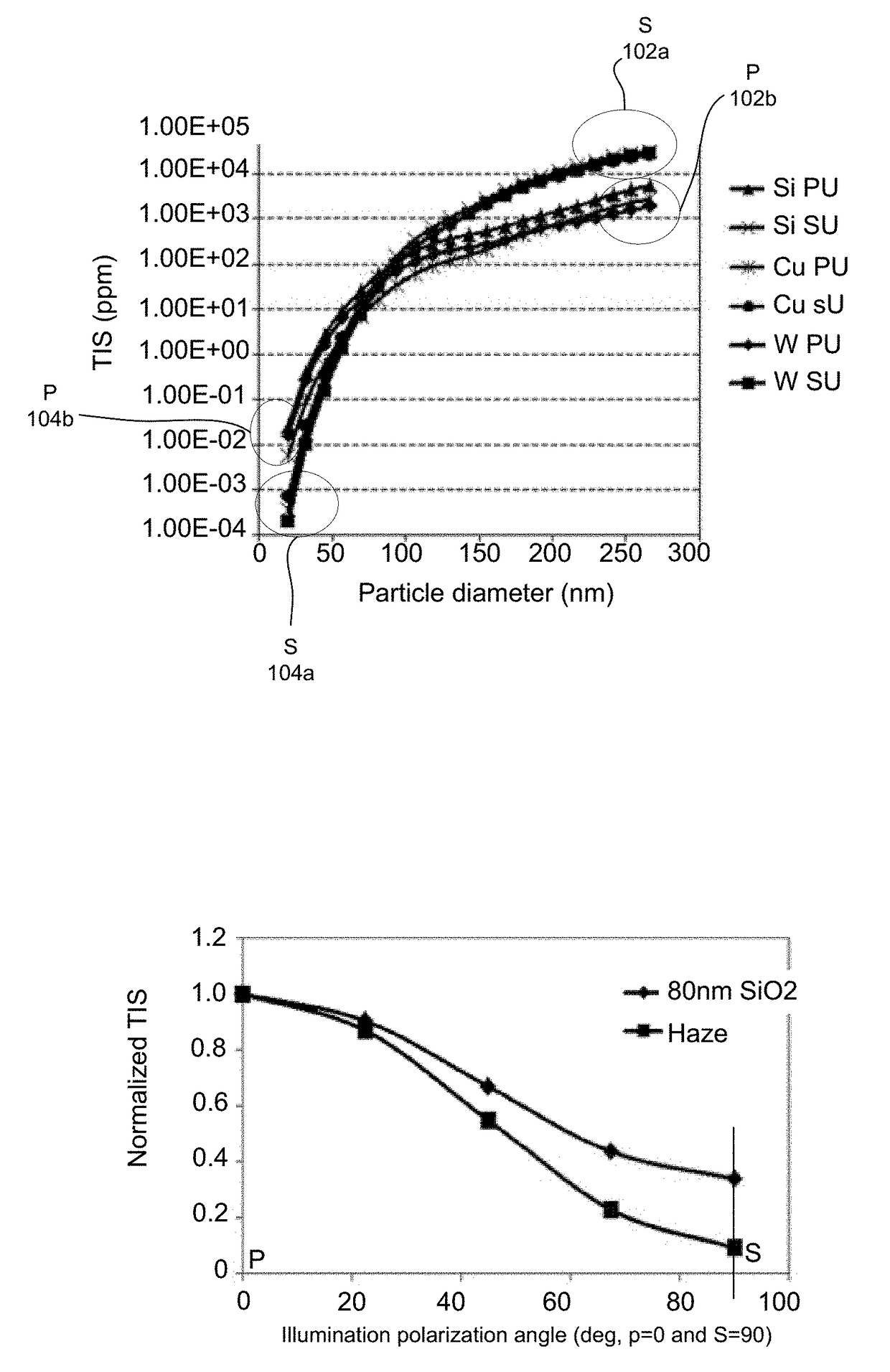
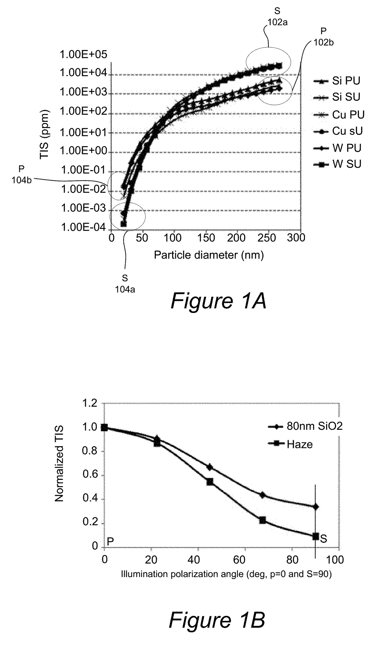
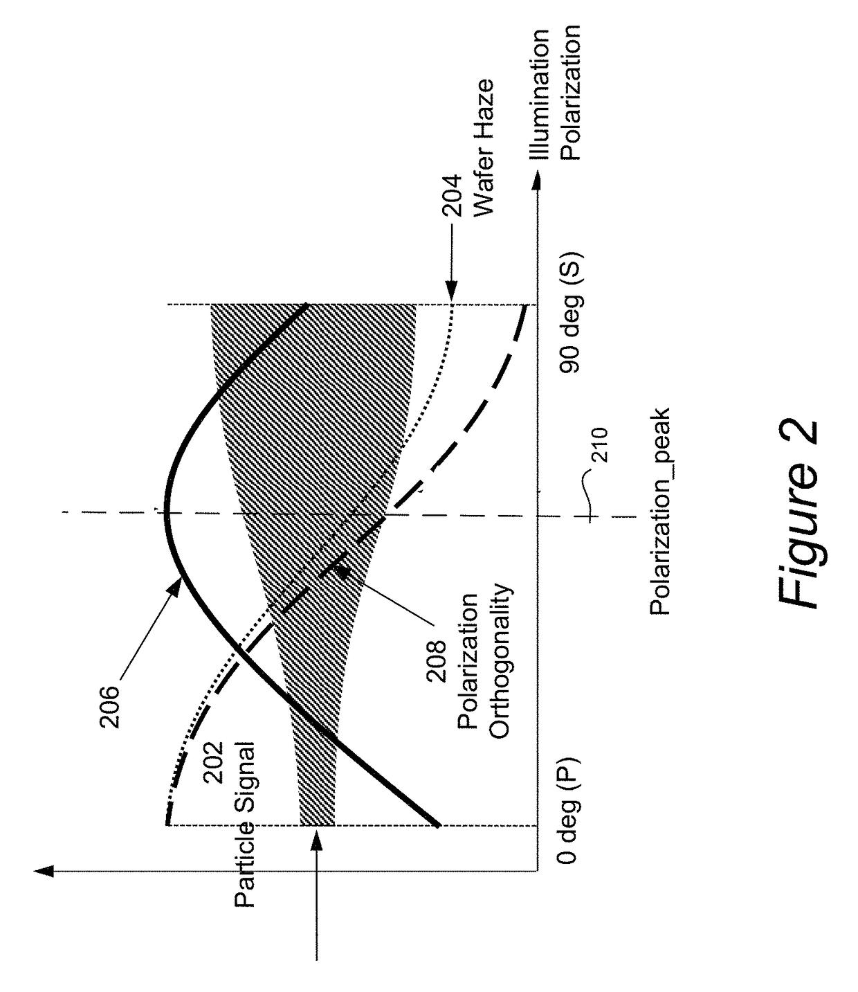
[0038]A semiconductor wafer inspection can sometimes use an inspection tool that is configurable to have a linearly polarized light configuration...


PUM

PropertyMeasurementUnit
particle diameteraaaaaaaaaa
defects sizesaaaaaaaaaa
semiconductoraaaaaaaaaa

Abstract

Disclosed are methods and apparatus for inspecting a semiconductor sample. This system comprises an illumination optics subsystem for generating and directing an incident beam towards a defect on a surface of a wafer. The illumination optics subsystem includes a light source for generating the incident beam and one or more polarization components for adjusting a ratio and / or a phase difference for the incident beam's electric field components. The system further includes a collection optics subsystem for collecting scattered light from the defect and / or surface in response to the incident beam, and the collection optics subsystem comprises an adjustable aperture at the pupil plane, followed by a rotatable waveplate for adjusting a phase difference of electric field components of the collected scattered light, followed by a rotatable analyzer. The system also includes a controller that is configured for (i) selecting a polarization of the incident beam, (ii) obtaining a defect scattering map, (iii) obtaining a surface scattering map, and (iv) determining a configuration of the one or more polarization components, aperture mask, and rotatable ¼ waveplate, and analyzer based on analysis of the defect and surface scattering map so as to maximize a defect signal to noise ratio,

Description

CROSS-REFERENCE TO RELATED APPLICATION[0001]This application claims priority to U.S. Provisional Patent Application No. 62 / 314,362, filed 28 Mar. 2016, which application is incorporated herein by reference in its entirety for all purposes.TECHNICAL FIELD OF THE INVENTION[0002]The invention generally relates to the field of wafer inspection systems. More particularly the present invention relates to defect detection.BACKGROUND[0003]Generally, the industry of semiconductor manufacturing involves highly complex techniques for fabricating integrating circuits using semiconductor materials which are layered and patterned onto a substrate, such as silicon. Due to the large scale of circuit integration and the decreasing size of semiconductor devices, the fabricated devices have become increasingly sensitive to defects. That is, defects which cause faults in the device are becoming increasingly smaller. The device needs to be generally fault free prior to shipment to the end users or custo...

Claims


Application Information

Patent Timeline
Patent Type & Authority Applications(United States)
IPC IPC(8): G01N21/88G01N21/95G01N21/21
CPCG01N21/8806G01N21/21G01N2201/0683G01N2021/8848G01N21/9501H01L22/12H01L22/20H01L22/30
Inventor LIU, SHENGZHAO, GUOHENG
Owner KLA CORP
Why Eureka
Try Eureka