Semiconductor device and manufacturing method thereof

a semiconductor device and manufacturing method technology, applied in non-linear optics, instruments, optical elements, etc., can solve the problems and achieve the effect of increasing the manufacturing cost of the semiconductor devi

Active Publication Date: 2017-10-05
RENESAS ELECTRONICS CORP
View PDF3 Cites 2 Cited by
  • Summary
  • Abstract
  • Description
  • Claims
  • Application Information

AI Technical Summary

Benefits of technology

[0007]The semiconductor device in which the heater is formed above the optical waveguide formed in a part of the SOI substrate as described above has a problem of the ...

Problems solved by technology

The semiconductor device in which the heater is formed above the optical waveguide formed in a part of the SOI substrate as described above has a problem of the inc...

Method used


Image

  • Semiconductor device and manufacturing method thereof
  • Semiconductor device and manufacturing method thereof
  • Semiconductor device and manufacturing method thereof

Examples


first embodiment

[0046]

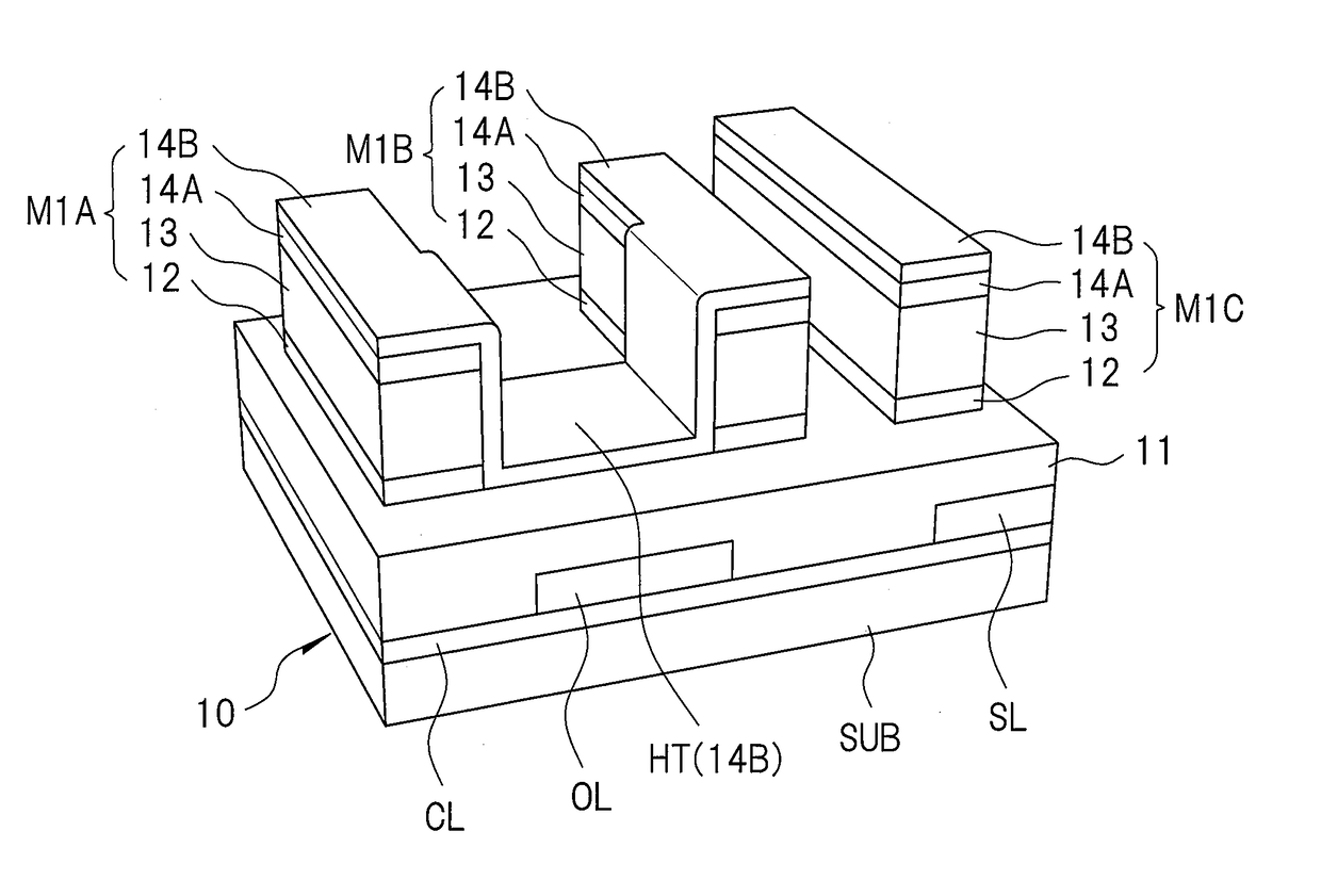
[0047]A structure of a semiconductor device according to the first embodiment will be described with reference to FIG. 1. FIG. 1 is a cross-sectional view showing a principal part of the semiconductor device according to the first embodiment.

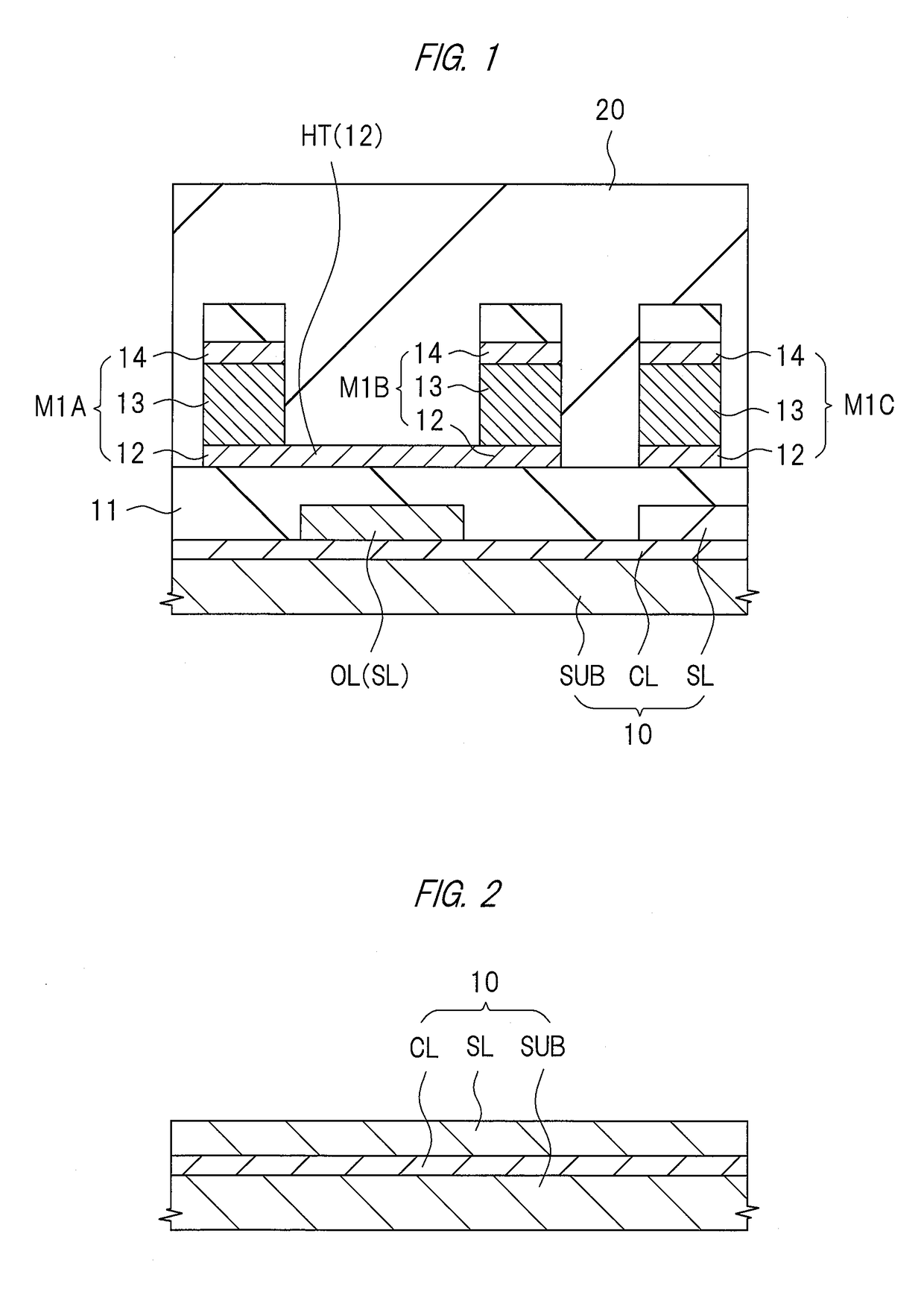
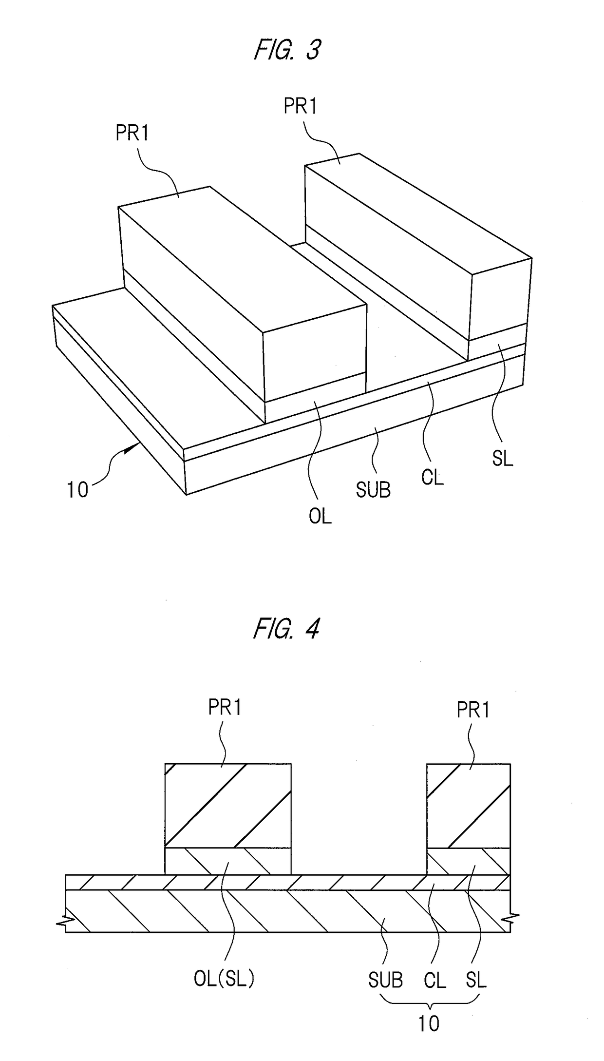
[0048]The semiconductor device includes an SOI substrate 10 constituted of a support substrate SUB made of single crystal silicon, a silicon oxide layer (referred to also as BOX layer or cladding layer) CL formed over the support substrate SUB and a semiconductor layer (referred to also as SOI layer) SL made of single crystal silicon formed over the silicon oxide layer CL. The SOI substrate 10 can be formed by, for example, the SIMOX (Silicon Implanted Oxide) method, the bonding method and the smart-cut method. As an example, a thickness of the support substrate SUB is about 750 μm, a thickness of the silicon oxide layer CL is about 2 μm, and a thickness of the semiconductor layer SL is about 200 nm.

[0049]An optical waveguide OL for transm...

second embodiment

[0075]In the first embodiment described above, the bottom barrier metal film 12 constituting a part of the wiring material is used to form the heater HT. Meanwhile, in the second embodiment, a bottom barrier metal film and a top barrier metal film constituting a part of a wiring material are used to form the heater HT.

[0076]Hereinafter, a manufacturing method of a semiconductor device according to the second embodiment will be described in the order of processes with reference to FIG. 15 to FIG. 26.

[0077]First, as shown in FIG. 15 and FIG. 16, the optical waveguide OL made of the semiconductor layer SL is formed in a part of the SOI substrate 10, and the silicon oxide film 11 is deposited over the optical waveguide OL and the semiconductor layer SL. Thereafter, the wiring material (bottom barrier metal film 12, aluminum-copper alloy film 13 and first top barrier metal film 14A) is deposited over the silicon oxide film 11.

[0078]The process up to the deposition of the silicon oxide fi...

third embodiment

[0089]In the first embodiment described above, the bottom barrier metal film 12 constituting a part of the wiring material is used to form the heater HT, and in the second embodiment, the laminated film of the bottom barrier metal film 12 and the second top barrier metal film 14B constituting a part of the wiring material is used to form the heater HT. Meanwhile, in the third embodiment, a top barrier metal film is used to form the heater HT.

[0090]Hereinafter, a manufacturing method of a semiconductor device according to the third embodiment will be described in the order of processes with reference to FIG. 27 to FIG. 32.

[0091]First, as shown in FIG. 27 and FIG. 28, in accordance with the same process as that shown in FIG. 15 to FIG. 18 of the second embodiment described above, the wiring material (bottom barrier metal film 12, aluminum-copper alloy film 13 and first top barrier metal film 14A) is deposited over the silicon oxide film 11, and then the photoresist film PR4 is formed ...


PUM


Abstract

An optical waveguide for optical signals is formed in a semiconductor layer of an SOI substrate, a heater for heating the optical waveguide is formed on a silicon oxide film which covers the optical waveguide, and wirings for supplying power to the heater are connected to both ends of the heater. Each of the wirings is constituted of a laminated film of a bottom barrier metal film, an aluminum-copper alloy film serving as a main conductive film and a top barrier metal film, and the heater is constituted integrally with the bottom barrier metal film constituting a part of each of the wirings.

Description

CROSS-REFERENCE TO RELATED APPLICATION[0001]The present application claims priority from Japanese Patent Application No. 2016-070284 filed on Mar. 31, 2016, the content of which is hereby incorporated by reference into this application.TECHNICAL FIELD OF THE INVENTION[0002]The present invention relates to a semiconductor device and a manufacturing method of the semiconductor device, and can be effectively utilized for, for example, a semiconductor device including an SOI (Silicon On Insulator) substrate in which an optical waveguide made of silicon (Si) is formed and manufacture of the semiconductor device.BACKGROUND OF THE INVENTION[0003]In recent years, the development of the so-called silicon photonics technology to realize an optical communication module by forming optical waveguides (optical signal transmission paths) made of silicon (Si) in a part of a silicon substrate and integrating optical circuits and electronic devices constituted of the optical waveguides has been activ...

Claims


Application Information

Patent Timeline
IPC IPC(8): H01L27/12H01L21/84G02B6/132H01L21/3213H01L21/311H01L21/48H01L23/34H01L23/538
CPCH01L27/1203H01L23/345H01L21/84H01L23/5386G02B2006/12061H01L21/31111H01L21/4853G02B6/132H01L21/32139G02F1/011G02B2006/12142
Inventor USAMI, TATSUYA
Owner RENESAS ELECTRONICS CORP
Why Eureka
Try Eureka