Dynamic wafer leveling/tilting/swiveling during a chemical vapor deposition process

a chemical vapor deposition and leveling technology, applied in the field of semiconductor manufacturing, can solve the problems of low temperature of such cvd processes and still exist deposition non-uniformities, and achieve the effects of reducing the difference in deposition non-uniformities, and reducing the difference in thickness

Active Publication Date: 2017-10-26
APPLIED MATERIALS INC
View PDF0 Cites 194 Cited by
  • Summary
  • Abstract
  • Description
  • Claims
  • Application Information

AI Technical Summary

Benefits of technology

[0007]The implementations described herein generally relate to the dynamic, real-time control of the process spacing between a substrate support and a gas distribution medium during a deposition process. Multiple dimensional degrees of freedom are utilized to change the angle and spacing of the substrate plane with respect to the gas distributing medium at any time during the deposition process. As such, the substrate and / or substrate support may be leveled, tilted, swiveled, wobbled, and / or moved during the deposition process to achieve improved film uniformity. Furthermore, the independent tuning of each layer may be had due to continuous variations in the leveling of the substrate plane with respect to the showerhead to average effective deposition on the substrate, thus improving overall stack deposition performance.
[0009]In another embodiment, a method of controlling processing spacing between a gas distribution medium and a substrate support disposed opposite the gas distribution medium is disclosed. The method includes adjusting the substrate support at a first mounting location coupled to the substrate support, and adjusting the substrate support at a second mounting location coupled to the substrate support. The adjusting of the substrate support at the first mounting location and at the second mounting location occurs during a chemical vapor deposition process and in real time to reduce a difference in deposition non-uniformities.
[0010]In yet another embodiment, a method of controlling processing spacing between a gas distribution medium and a substrate support disposed opposite the gas distribution medium is disclosed. The method includes (a) depositing a layer on a substrate disposed on the substrate support, (b) measuring a thickness of the layer on the substrate, and (c) calculating differences in thickness between a reference location on the substrate and a plurality of remaining locations on the substrate. The method also includes (d) determining processing spacing adjustment amounts for the plurality of remaining locations relative to the reference location based on the differences in thickness between the reference location and the plurality of remaining locations, and (e) dynamically adjusting the substrate support in real time at a first mounting location coupled to the substrate support to reduce the differences in thickness between the reference location and each of the plurality of remaining locations. The method also includes (f) dynamically adjusting the substrate support in real time at a second mounting location coupled to the substrate support to reduce the differences in thickness between the reference location and each of the plurality of remaining locations, wherein each dynamic adjusting occurs during the depositing.

Problems solved by technology

The high reactivity of the released species reduces the energy needed for a chemical reaction to take place, and thus lowers the temperature for such CVD processes.
However, deposition non-uniformities still exist even with restricted movement of the substrate during deposition.

Method used


Image

  • Dynamic wafer leveling/tilting/swiveling during a chemical vapor deposition process
  • Dynamic wafer leveling/tilting/swiveling during a chemical vapor deposition process
  • Dynamic wafer leveling/tilting/swiveling during a chemical vapor deposition process

Examples


Embodiment Construction

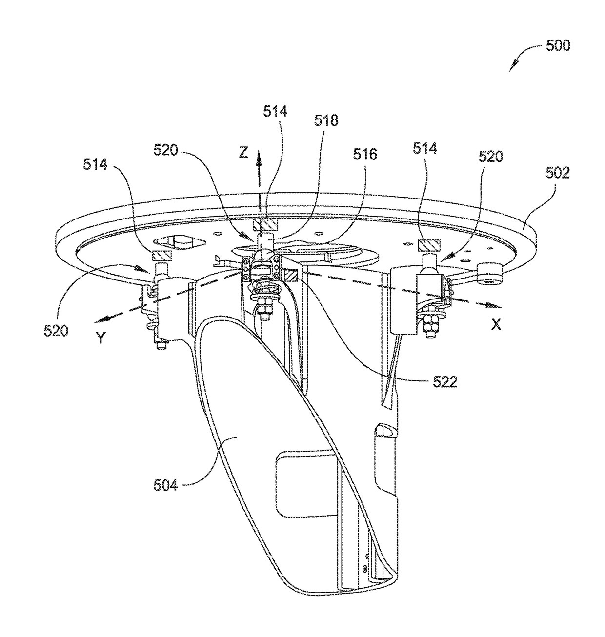
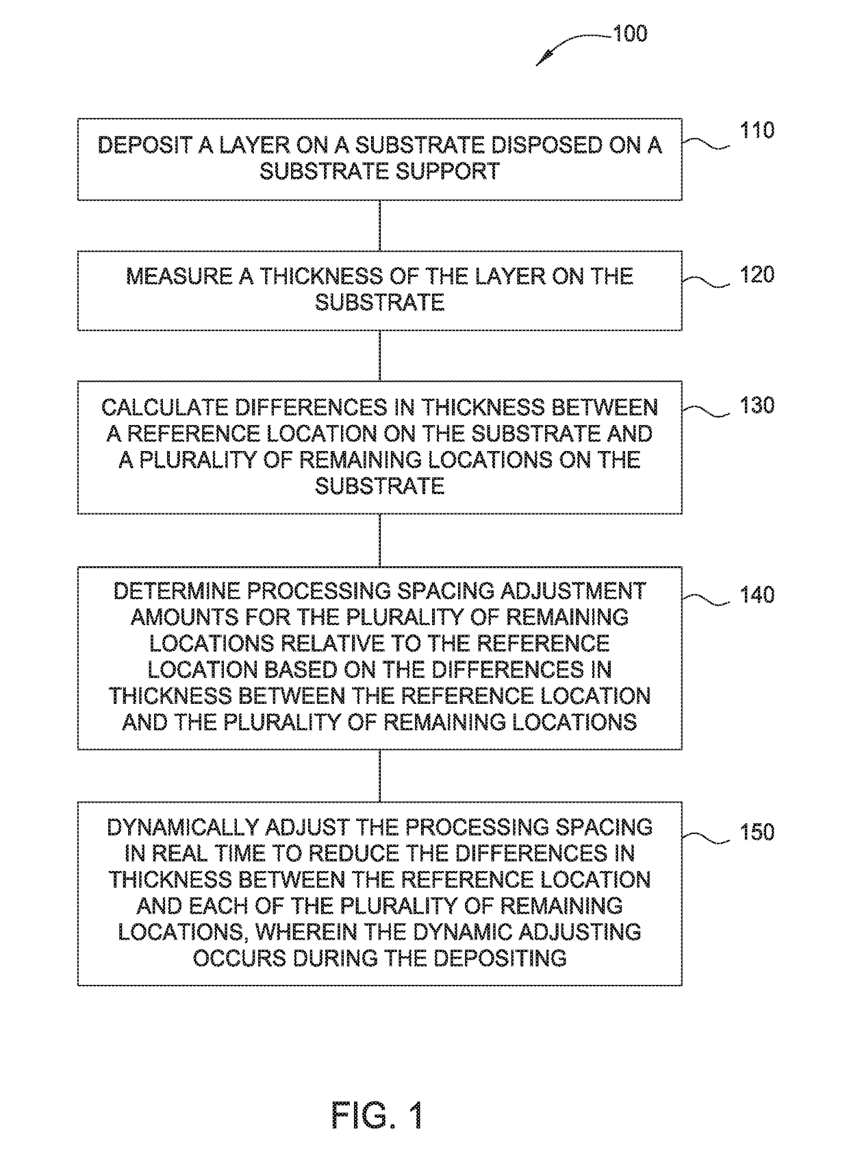
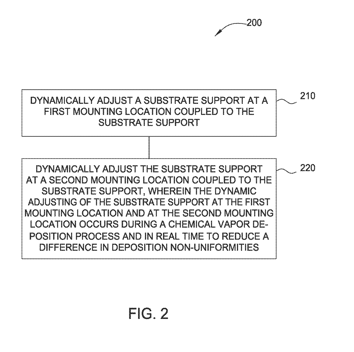
[0018]The implementations described herein generally relate to the dynamic, real-time control of the process spacing between a substrate support and a gas distribution medium during a deposition process. Multiple dimensional degrees of freedom are utilized to change the angle and spacing of the substrate plane with respect to the gas distributing medium at any time during the deposition process. As such, the substrate and / or substrate support may be leveled, tilted, swiveled, wobbled, and / or moved during the deposition process to achieve improved film uniformity. Furthermore, the independent tuning of each layer may occur due to continuous variations in the leveling of the substrate plane with respect to the showerhead to average effective deposition on the substrate, thus improving overall stack deposition performance.

[0019]A “substrate” or “substrate surface,” as described herein, generally refers to any substrate surface upon which processing is performed. For example, a substrat...


PUM

PropertyMeasurementUnit
temperatureaaaaaaaaaa
thicknessaaaaaaaaaa
processing spacingaaaaaaaaaa

Abstract

The implementations described herein generally relate to the dynamic, real-time control of the process spacing between a substrate support and a gas distribution medium during a deposition process. Multiple dimensional degrees of freedom are utilized to change the angle and spacing of the substrate plane with respect to the gas distributing medium at any time during the deposition process. As such, the substrate and / or substrate support may be leveled, tilted, swiveled, wobbled, and / or moved during the deposition process to achieve improved film uniformity. Furthermore, the independent tuning of each layer may be had due to continuous variations in the leveling of the substrate plane with respect to the showerhead to average effective deposition on the substrate, thus improving overall stack deposition performance.

Description

BACKGROUNDField[0001]Implementations of the present disclosure generally relate to semiconductor manufacturing and, more particularly, to methods and apparatus for achieving a desired thickness uniformity of a layer formed on a substrate during a deposition process.Description of the Related Art[0002]The fabrication of semiconductor devices involves the formation of a thin film on a semiconductor substrate by a chemical reaction of gases. Such a deposition process is referred to as chemical vapor deposition (CVD). Conventional thermal CVD processes supply reactive gases to the substrate surface where heat-induced chemical reactions can take place to produce the desired film. Plasma enhanced CVD processes promote the excitation and / or dissociation of the reactant gases by the application of energy, such as radio frequency (RF) energy, to the reaction zone proximate the substrate surface thus creating a plasma of highly reactive species. The high reactivity of the released species red...

Claims


Application Information

Patent Timeline
Patent Type & Authority Applications(United States)
IPC IPC(8): H01L21/66H01L21/285H01L21/02H01L21/687
CPCH01L22/26H01L21/68785H01L21/28556H01L21/0262H01L21/02271C23C16/45565C23C16/45589C23C16/4583C23C16/52H01L22/12H01L21/67253H01L21/68742H01L21/68764H01L21/205H01L21/02274H01L21/0228
Inventor BANSAL, AMIT KUMARROCHA-ALVAREZ, JUAN CARLOSJANAKIRAMAN, KARTHIKNGUYEN, TUAN ANH
Owner APPLIED MATERIALS INC
Why Eureka
Try Eureka