Integrated photonic polarisation rotator and splitter and related method

a photonic polarization and rotator technology, applied in the direction of instruments, optical light guides, optical waveguide light guides, etc., can solve the problems of several impairments in the optical transmission system, one of the trickiest problems in polarization handling, etc., and achieve the effect of compact devices

Active Publication Date: 2017-11-02
CONSORZIO NAZI INTERUNIV PER LE TELECOMM (CNIT) +1
View PDF1 Cites 7 Cited by
  • Summary
  • Abstract
  • Description
  • Claims
  • Application Information

AI Technical Summary

Benefits of technology

[0041]According to the principle underlying the present invention to overcome the drawbacks mentioned with refe...

Problems solved by technology

Polarization handling is one of the trickiest issues in Silicon Photonics.
Due to the intrinsic high birefringence of the High index contrast waveguides,...

Method used


Image

  • Integrated photonic polarisation rotator and splitter and related method
  • Integrated photonic polarisation rotator and splitter and related method
  • Integrated photonic polarisation rotator and splitter and related method

Examples


example

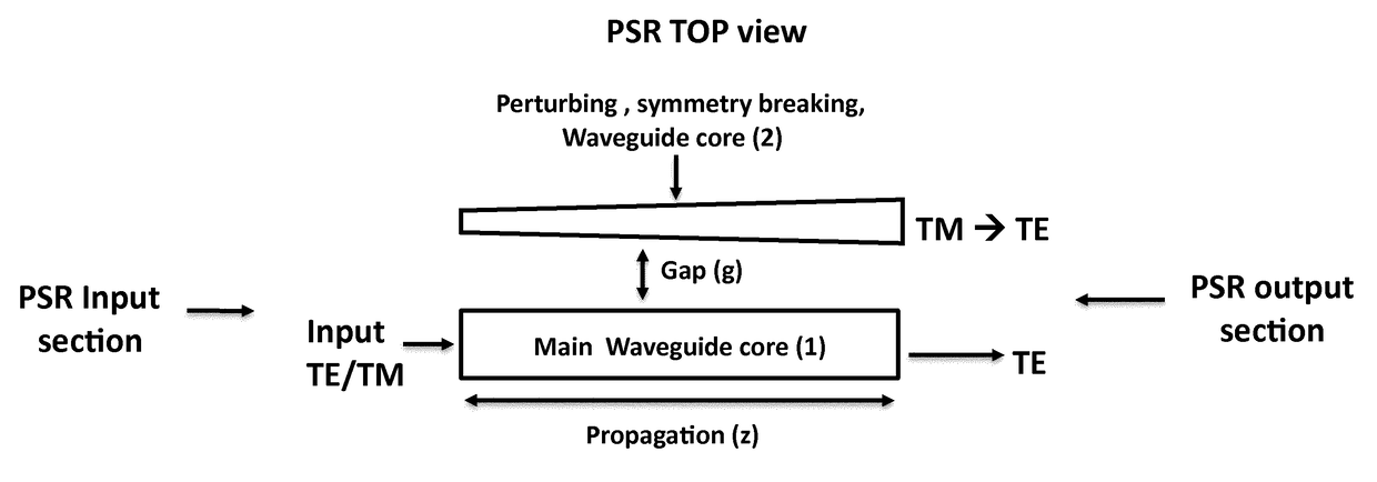
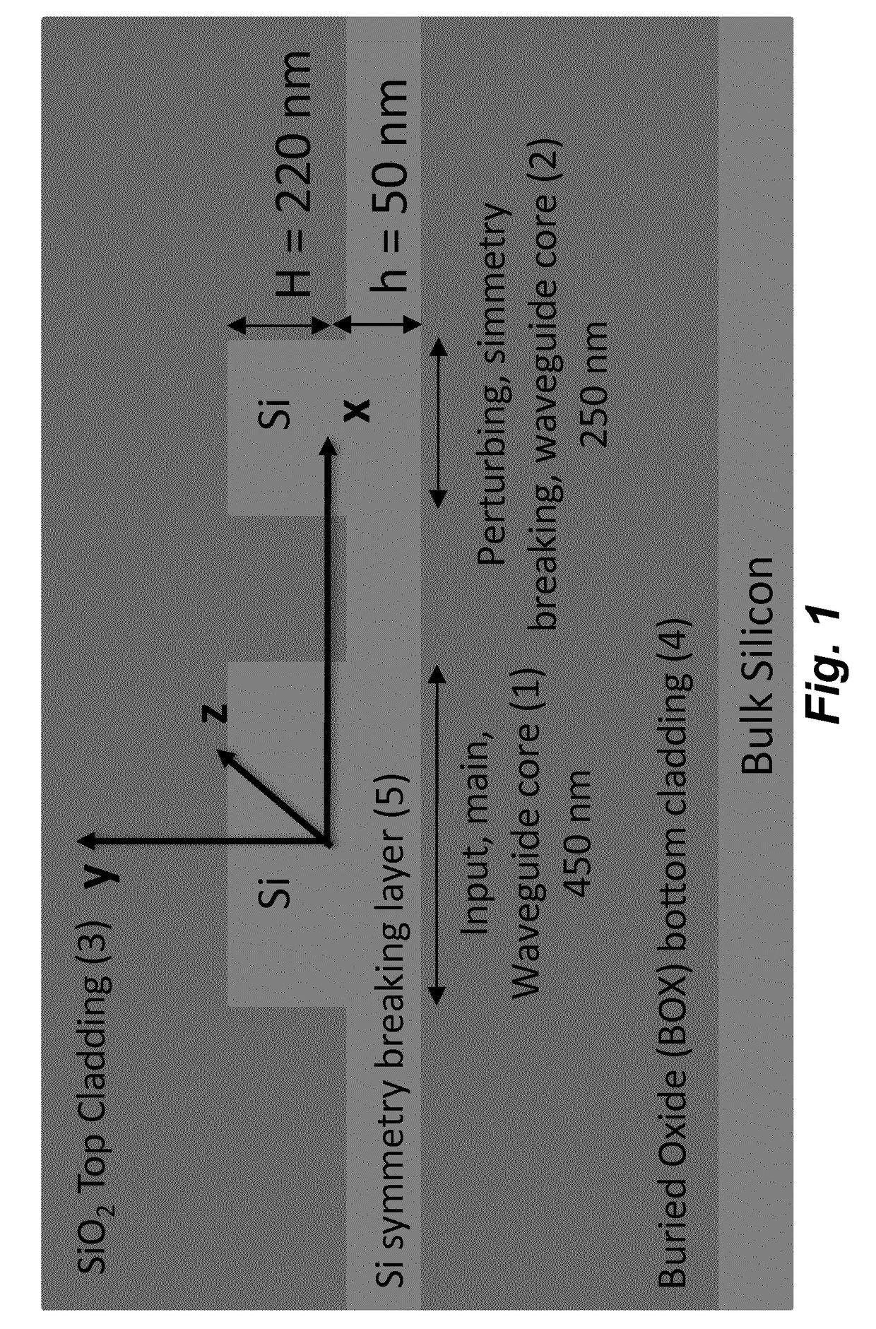
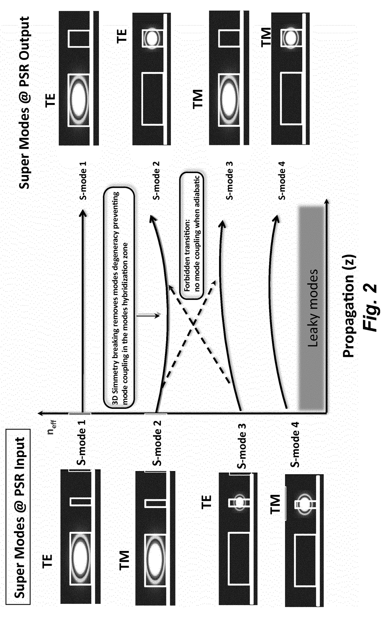
[0179]For a full illustration of the photonic device design and functioning, reference is made to FIG. 10. A 50 nm thick Poly-Si layer is in contact, or in close proximity, to the 220 nm thick Si layer of an SOI wafer or, alternatively, an all Si ridge waveguide can be used (not shown here). Said Poly-Si layer is unetched and extends through the entire device length continuously breaking the vertical symmetry with respect to the main waveguide. At the same time, symmetry is also continuously broken in the horizontal direction by the Si perturbing waveguide. Main and perturbing waveguides are separated by a 150 nm gap constant throughout the entire device length. A SiO2 top cladding is used. A scrambled TE / TM signal is inputted in the 450 nm wide Si waveguide which is single mode for each polarization at λ=1.5 μm. The PSR length is 150 μm. A 25 μm long adiabatic transition is used to bring the main and perturbing waveguides in close proximity and a 50 μm long adiabatic one to separat...


PUM


Abstract

In an integrated polarization splitting and rotating photonic device comprising at least one first waveguide; a second waveguide, both said waveguides extending from an input section to an output section; a top cladding; a bottom cladding and a symmetry-breaking layer so as to form an optical guiding structure in a wafer chip, said top and bottom claddings extending throughout the whole optical guiding structure sandwiching said waveguides therebetween, said symmetry-breaking layer extends in the optical guiding structure at least over the whole guiding structure length, and, at the input section, the at least one first waveguide core has a predetermined width through the optical guiding structure to the output section, receiving an input light signal, and further, the second waveguide core, both at the input and the output section, has a width narrower than said predetermined width of the first waveguide core; so that the optical guiding structure guides a first mode substantially confined within said at least one first waveguide core and a second mode substantially confined within said second semiconductor waveguide core said first and said second modes having the same polarization at the output section.

Description

BACKGROUND OF THE INVENTION1. Field of the Invention[0001]The present invention concerns an integrated photonic device, in particular an integrated polarization splitting and rotating photonic device to be implemented in a wafer chip. This kind of device is conceived to receive through an optical fibre a light input, to manage the polarization thereof.[0002]More specifically, the invention refers to a polarization and rotating photonic device, commonly referred as PSR device also in the following, comprising at least one first waveguide core, a second waveguide core, both said waveguide cores extending from an input section to an output section and being separated by a gap at least at the output section, a top cladding and a bottom cladding, said claddings extending along the whole optical guiding structure enclosing said waveguides there between, so as to form an optical guiding structure in a chip.2. Description of the Prior Art[0003]Polarization handling is one of the trickiest i...

Claims


Application Information

Patent Timeline
IPC IPC(8): G02B6/126G02B6/122G02B6/12
CPCG02B6/126G02B2006/12116G02B6/1228G02B6/14
Inventor SOCCI, LUCIANOROMAGNOLI, MARCO
Owner CONSORZIO NAZI INTERUNIV PER LE TELECOMM (CNIT)
Why Eureka
Try Eureka