Thermal infrared detector and manufacturing method for thermal infrared detector

a manufacturing method and detector technology, applied in the direction of pyrometry using electric radation detectors, optical radiation measurement, instruments, etc., can solve the problems of difficult to improve the sensitivity, the aperture of the sensor element decreases, and the character deteriorates dramatically, so as to improve the detection sensitivity, reduce the thermal time constant, and increase the aperture

Active Publication Date: 2017-11-16
MITSUBISHI ELECTRIC CORP
View PDF10 Cites 9 Cited by
  • Summary
  • Abstract
  • Description
  • Claims
  • Application Information

AI Technical Summary

Benefits of technology

[0009]In consideration of the circumstances described above, the prior art described in Japanese Patent No. 4224949 improves the sensitivity of a thermal infrared detector by providing an infrared ray absorption structure on an upper portion of the sensor element in order to increase the aperture thereof. With a structure such as that described in Japanese Patent No. 4224949, however, an etching hole through which the sensor element is hollowed out and thereby thermally insulated must be provided in the infrared ray absorption structure. As a result, the aperture decreases.
[0018]According to this invention, there is no need to provide an etching hole in the sensor element, and therefore the aperture can be increased. Moreover, the trench structure provided between the sensor elements remains connected to the substrate even after heat insulation hollowing processing, and therefore a structure that functions as a beam for supporting the pixel area is provided. As a result, a thermal infrared detector structured such that an improvement in detection sensitivity, a reduction in a thermal time constant, and an improvement in the physical strength of a pixel area can be realized, as well as a manufacturing method for the thermal infrared detector, can be obtained.

Problems solved by technology

However, the prior art includes the following problems.
As a result, a sensor characteristic deteriorates dramatically, making it difficult to improve the sensitivity even by providing an infrared ray absorption structure in order to increase the aperture.
In Japanese Patent No. 3944465, however, the aperture of the sensor element decreases due to light blockage by the heat insulation support leg provided on the sensor element.

Method used


Image

  • Thermal infrared detector and manufacturing method for thermal infrared detector
  • Thermal infrared detector and manufacturing method for thermal infrared detector
  • Thermal infrared detector and manufacturing method for thermal infrared detector

Examples


first embodiment

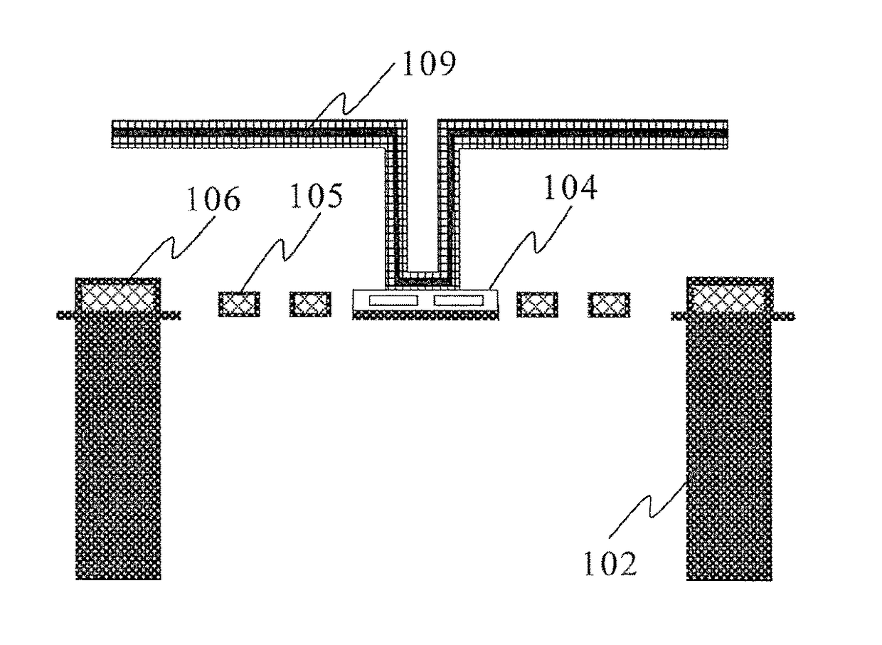
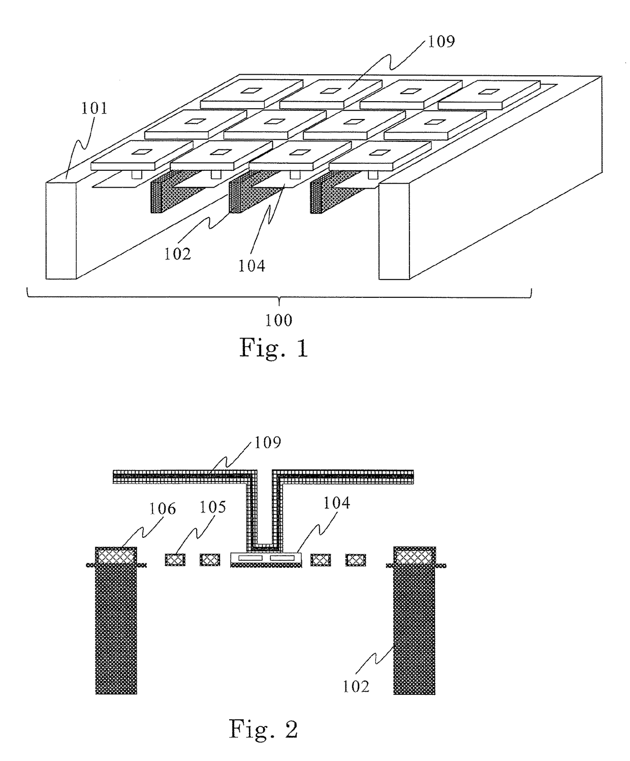
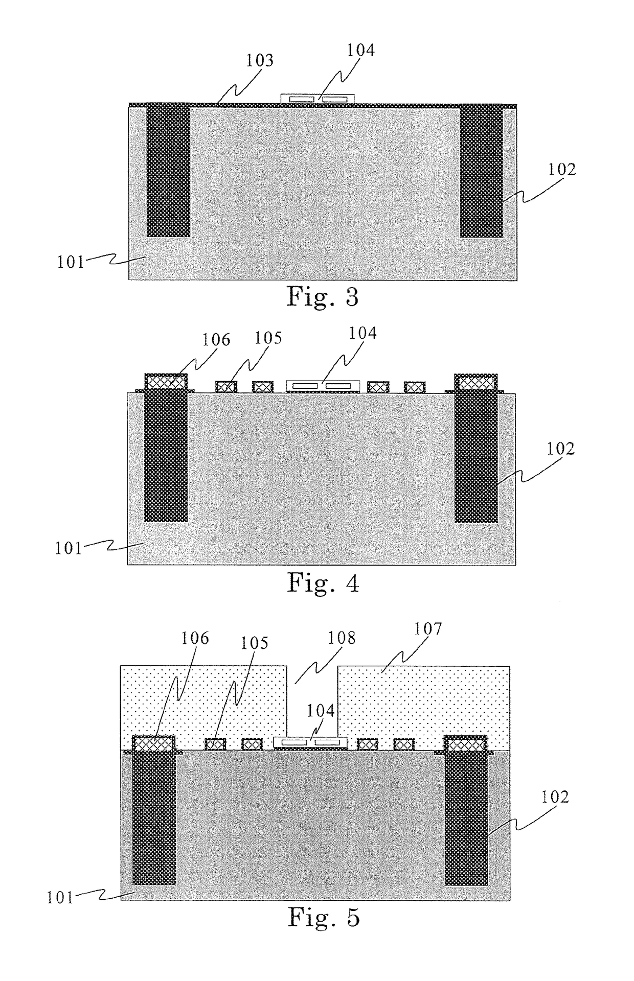
[0060]FIG. 1 is a bird's-eye view showing a thermal infrared detector according to a first embodiment of this invention, and FIG. 2 is a sectional view of the thermal infrared detector according to the first embodiment of this invention. A thermal infrared detector 100 shown in FIGS. 1 and 2 is configured to include a substrate 101, a trench structure 102, a sensor element 104, a heat insulation support leg 105, a wire 106, and an infrared ray absorption structure 109.

[0061]In the thermal infrared detector 100 according to the first embodiment, heat insulation hollowing processing is performed without providing an etching hole in the infrared ray absorption structure 109. The thermal infrared detector 100 therefore has a larger aperture than the thermal infrared detector described in Japanese Patent No. 4224949, and as a result, the sensitivity of the thermal infrared detector can be improved.

[0062]Moreover, the trench structures 102 provided between the sensor elements remain conne...

second embodiment

[0082]In a second embodiment of this invention, a thermal infrared detector in which a thermal resistance of the wire 106 for connecting the sensor element to the peripheral circuit can be reduced, enabling a reduction in a thermal time constant, by embedding a high thermal conductivity material 202 in a trench structure 203 will be described.

[0083]Processes for manufacturing the thermal infrared detector according to the second embodiment will be described in sequence using FIGS. 11 to 18. FIGS. 11 to 18 are views showing a sequence of processes for manufacturing the thermal infrared detector according to the second embodiment of this invention.

[0084]Note that FIGS. 13 to 18 show similar processes to the first embodiment, and therefore detailed description thereof has been omitted. Accordingly, in the second embodiment described below, only structures that are unique to the second embodiment and effects derived therefrom will be described, while description of other structures that...

third embodiment

[0094]In a third embodiment of this invention, a thermal infrared detector in which an infrared ray absorbing film is formed additionally on the rear surface side of the sensor element will be described.

[0095]Newly added processes among processes for manufacturing the thermal infrared detector according to the third embodiment will be described in sequence below using FIGS. 19 and 20. FIGS. 19 and 20 are views showing a sequence of processes for manufacturing the thermal infrared detector according to the third embodiment of this invention.

[0096]As shown in FIG. 19, following the process shown in FIG. 8 of the first embodiment or the process shown in FIG. 16 of the second embodiment, an infrared ray absorbing film 301 is formed on a rear surface of a wafer from vanadium, titanium, chrome, a Co-based compound, and a nitride or oxide thereof using a CVD method or the like.

[0097]Next, the infrared ray absorbing film 301 is removed from all regions apart from the region of the sensor el...


PUM


Abstract

In a thermal infrared detector having trench structures, at least one sensor element is provided between the trench structures, an etching hole through which the sensor element is hollowed out and thereby thermally insulated is provided in a substrate rear surface or on the periphery of a pixel area, and an opening portion is provided below the pixel area.

Description

BACKGROUND OF THE INVENTION1. Field of the Invention[0001]This invention relates to a thermal infrared detector that converts heat generated by infrared ray absorption into electricity and detects the electricity, and more particularly to a highly sensitive thermal infrared detector having a small thermal time constant, and a manufacturing method for manufacturing the thermal infrared detector with stability.2. Description of the Related Art[0002]Infrared detectors using infrared rays can be broadly divided according to operating principle into thermal infrared detectors that utilize temperature variation occurring when energy from the infrared rays is absorbed, and quantum infrared detectors that utilize carrier excitation resulting from absorption of the infrared rays.[0003]A quantum infrared detector operates at a low temperature, and therefore an element used thereby must be cooled to approximately −200° C. using a refrigerator. As a result, drawbacks such as structural complexi...

Claims


Application Information

Patent Timeline
Patent Type & Authority Applications(United States)
IPC IPC(8): G01J5/10G01J5/08
CPCG01J5/10G01J5/0809G01J2005/103G01J5/024G01J5/06G01J5/20G01J2005/065G01J5/0853G01J5/59
Inventor KOBAYASHI, SATOISUGINO, TAKAKIHARA, TAKAFUMIKAWANO, YUJI
Owner MITSUBISHI ELECTRIC CORP
Why Eureka
Try Eureka