Printed circuit board and optical module
- Summary
- Abstract
- Description
- Claims
- Application Information
AI Technical Summary
Benefits of technology
Problems solved by technology
Method used
Image
Examples
first embodiment
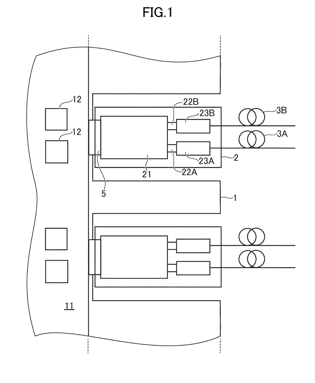
[0072]FIG. 1 is a schematic view for illustrating the configurations of a transmission device 1 and an optical module 2 according to a first embodiment of the present invention. The transmission device 1 includes a printed circuit board 11. Further, the optical module 2 includes a printed circuit board 21. One or both of those printed circuit boards 11 and 21 correspond to a printed circuit board according to the first embodiment.
[0073]The transmission device 1 further includes ICs 12. The transmission device 1 is, for example, a router or a switch having large capacity. The transmission device 1 has, for example, the function of a switch, and is installed in a base station or the like. The transmission device 1 obtains reception data (reception electric signal) by the optical module 2, and determines the destination and type of data to be transmitted, with the use of the IC 12 and the like. Then, the transmission device 1 generates transmission data (transmission electric signal), ...
second embodiment
[0136]FIG. 6A and FIG. 6B are schematic plan views for illustrating part of the structure of a printed circuit board 42 according to a second embodiment of the present invention. The printed circuit board 42 according to the second embodiment has the same structure as that of the printed circuit board 31 according to the first embodiment except that the shapes and dimensions of a differential transmission line included in the printed circuit board 42 according to the second embodiment differ from those of the first embodiment. The optical module 2 according to the second embodiment includes the printed circuit board 42 as the printed circuit board 21. A desired differential impedance can be obtained by increasing or reducing the gap Gap illustrated in FIG. 6B. Here, it is described that connection having satisfactory characteristics is achieved with at least a differential transmission line having a differential impedance value within a range of from 50Ω to 60Ω. The differential imp...
third embodiment
[0142]FIG. 8A and FIG. 8B are schematic plan views for illustrating part of the structure of a printed circuit board 43 according to a third embodiment of the present invention. FIG. 8C is a schematic cross-sectional view for illustrating part of the printed circuit board 43 according to the third embodiment. FIG. 8C is an illustration of a cross section taken along the line VIIIC-VIIIC of FIG. 8A. The printed circuit board 43 according to the third embodiment has the same structure as that of the printed circuit board 31 according to the first embodiment except for the following points. The shape of each of the plurality of conductor plate pairs 102 of a differential transmission line included in the printed circuit board 43 according to the third embodiment differs from that of the first embodiment. Correspondingly, the shapes of the first strip conductor pair 104, the second strip conductor pair 105, the first through hole 119, and the second through hole 129 differ from those of...
PUM
 Abstract
Description
Claims
Application Information


