Semiconductor device, system, and method for operating system

Active Publication Date: 2017-12-14
SEMICON ENERGY LAB CO LTD
View PDF0 Cites 0 Cited by
  • Summary
  • Abstract
  • Description
  • Claims
  • Application Information

AI Technical Summary

Benefits of technology

The patent text describes a semiconductor device that can display images using both light emitted from a light-emitting element and ambient light reflection. However, the driver circuits needed to drive these display panels can be large and lead to increased power consumption. The technical effects of this patent text are to provide a semiconductor device with a smaller circuit area and lower power consumption. This can be achieved by providing a novel semiconductor device that can display images using both functions while reducing the required driver circuits and power consumption. The semiconductor device can be used in various electronic devices and systems.

Problems solved by technology

Moreover, an increased number of driver circuits may result in higher power consumption of the display device.

Method used


Image

  • Semiconductor device, system, and method for operating system
  • Semiconductor device, system, and method for operating system
  • Semiconductor device, system, and method for operating system

Examples


embodiment 1

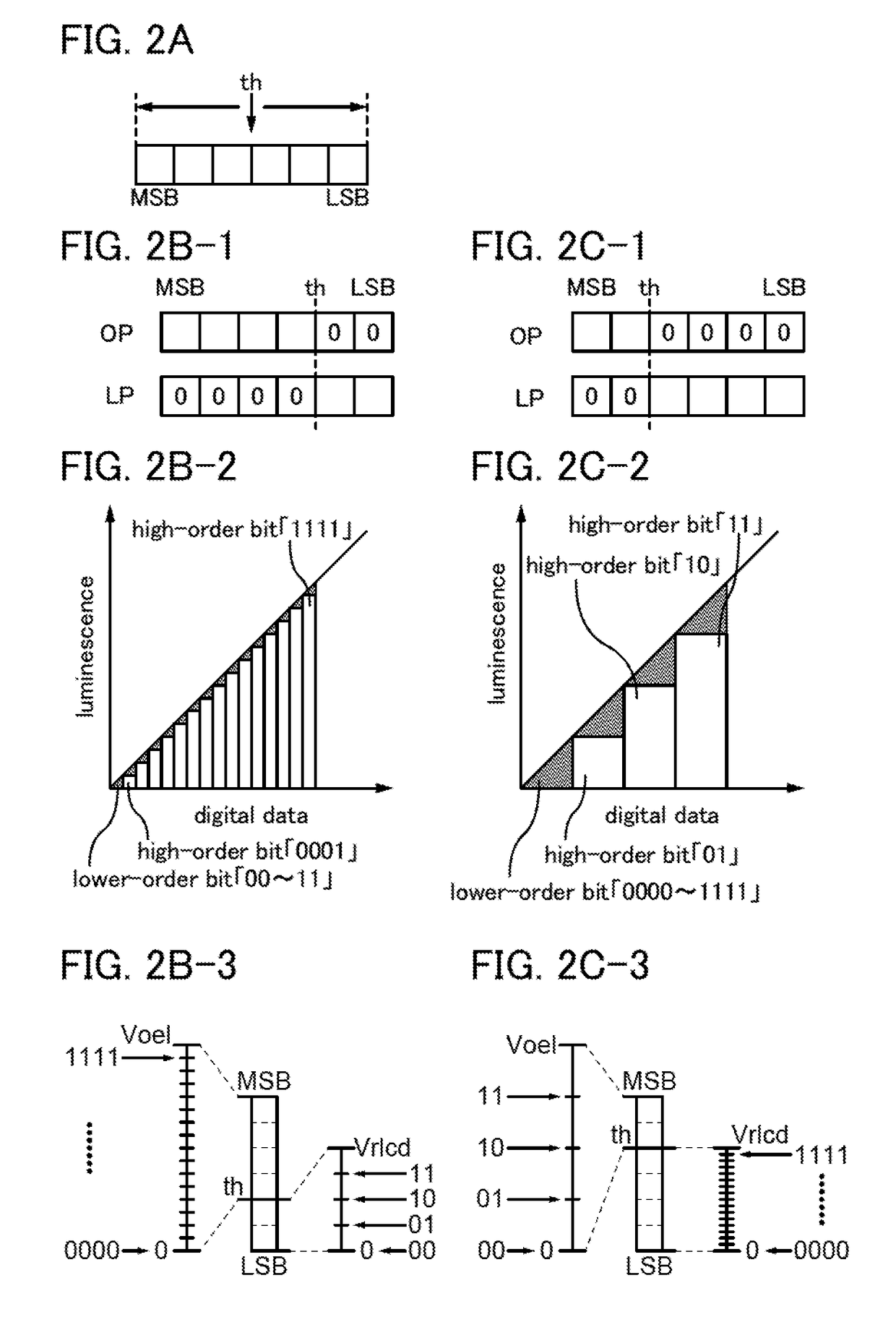
[0052]In this embodiment, an example of a semiconductor device that can be provided in a display device will be described.

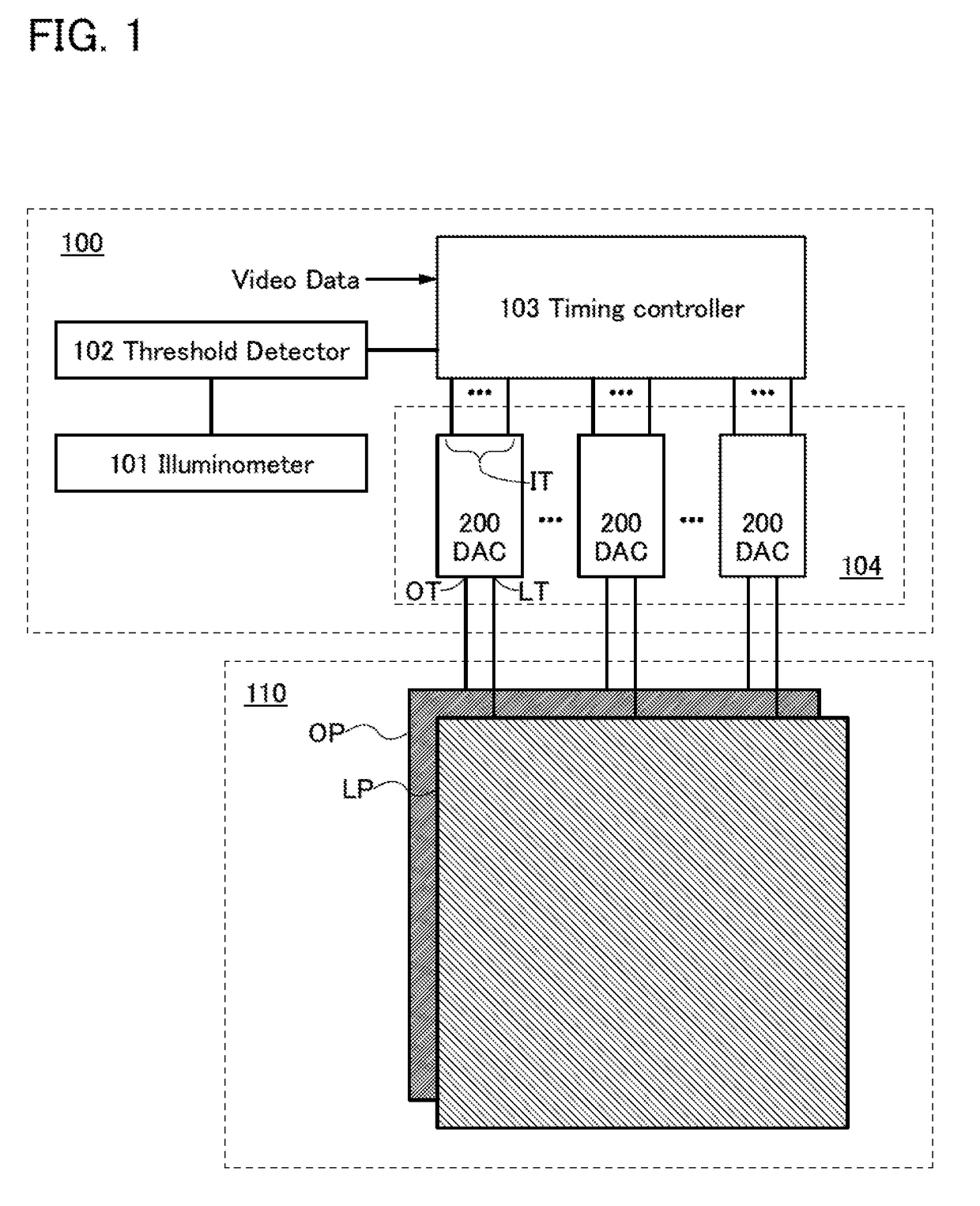
[0053]FIG. 1 illustrates an example of a display portion and a driver circuit portion that can be provided in a display device. A semiconductor device 100 illustrated in FIG. 1 is part of a source driver capable of driving a pixel circuit including a liquid crystal element and a pixel circuit including a light-emitting element. The semiconductor device 100 includes an illuminometer 101, a threshold-value detection circuit (hereinafter referred to as threshold detector) 102, a timing controller 103, and a circuit 104. The semiconductor device 100 is electrically connected to a display portion 110.

[0054]The display portion 110 includes a display panel LP and a display panel OP. The display panel LP can be, for example, a reflective liquid crystal panel including a liquid crystal element. The display panel OP can be a light-emitting device including a light-emitting...

embodiment 2

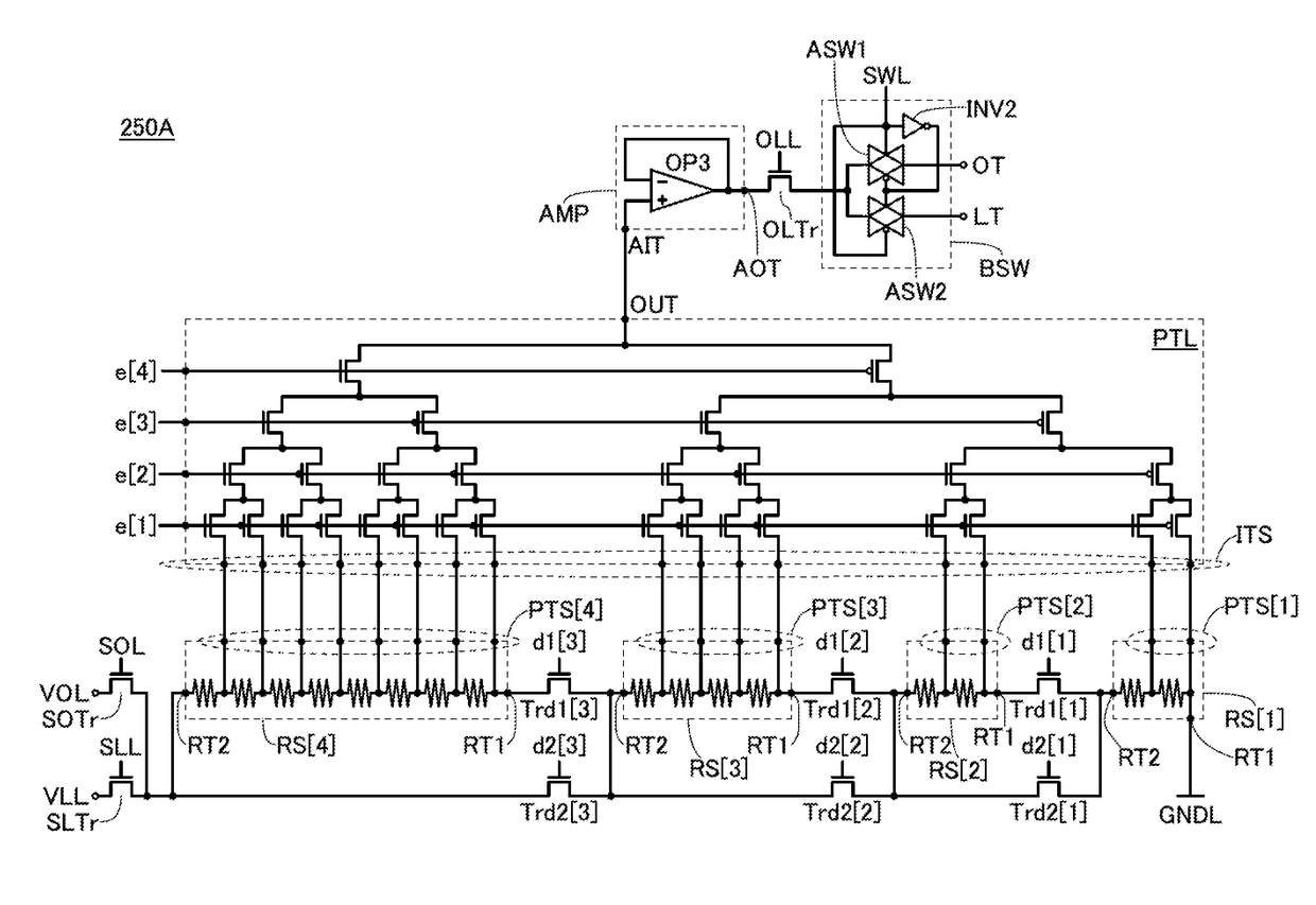
[0170]This embodiment will show an example where the semiconductor device described in Embodiment 1 is used in a source driver circuit.

[0171]FIG. 10 illustrates an example of a source driver circuit of one embodiment of the present invention. A source driver circuit 300 includes a low voltage differential signaling (LVDS) receiver 310, a serial-parallel converter circuit 320, a shift register circuit 330, a latch circuit 340, a level shifter 350, a circuit 360, a resistor string circuit 365, a pass transistor logic circuit 370, an external correction circuit 380, a band gap reference (BGR) circuit 390, a bias generator 400, and a buffer amplifier 500. Note that the number of bias generators 400 included in the source driver circuit 300 in FIG. 10 is two.

[0172]The LVDS receiver 310 is electrically connected to an external host processor. The LVDS receiver 310 has a function of receiving video signals from the host processor. Moreover, the LVDS receiver 310 converts a differential sig...

embodiment 3

[0187]Referring to FIGS. 11A to 11E, this embodiment will show an example where the semiconductor device described in the foregoing embodiment is used in an electronic component.

[0188]FIG. 11A shows an example in which the semiconductor device described in the foregoing embodiment is used as a memory device in an electronic component. Note that an electronic component is also referred to as a semiconductor package or an IC package. For the electronic component, there are various standards and names corresponding to the direction or the shape of terminals; hence, one example of the electronic component will be described in this embodiment.

[0189]The semiconductor device including transistors, capacitors, and the like, such as one described in Embodiment 1, is completed through an assembly process (post-process) of assembling detachable components on a printed board.

[0190]The post-process can be completed through steps shown in FIG. 11A. Specifically, after an element substrate obtaine...


PUM


Abstract

An object is to provide a semiconductor device that automatically adjusts the luminance of a display device. The semiconductor device includes an illuminometer, a threshold detector, a timing controller, a digital-to-analog converter circuit, a first display panel, and a second display panel. The illuminance of external light is measured with the illuminometer, and the threshold value of digital video data is determined by the threshold detector in accordance with the illuminance. The timing controller generates a signal for the first display panel or a signal for the second display panel on the basis of the threshold value and video data transmitted from the outside. The signal for the first display panel and the signal for the second display panel are input to one digital-to-analog converter circuit and converted into digital signals, and the obtained digital signals are input to a corresponding one of the first display panel and the second display panel.

Description

BACKGROUND OF THE INVENTION1. Field of the Invention[0001]One embodiment of the present invention relates to a semiconductor device, a system, and a method for operating the system.[0002]Note that one embodiment of the present invention is not limited to the above technical field. The technical field of the invention disclosed in this specification and the like relates to an object, a method, or a manufacturing method. In addition, one embodiment of the present invention relates to a process, a machine, manufacture, or a composition_of matter. Specific examples of the technical field of one embodiment of the present invention disclosed in this specification include a semiconductor device, a display device, a liquid crystal display device, a light-emitting device, a power storage device, an imaging device, a memory device, a processor, an electronic device, a method for driving any of them, a method for manufacturing any of them, a method for testing any of them, and a system includi...

Claims


Application Information

Patent Timeline
IPC IPC(8): G09G3/20G09G3/36H01L27/12G09G3/3225H03K19/08
CPCG09G3/2007H01L27/1225G09G3/3225G09G3/3648G09G2310/027G09G2300/0814G09G2300/0833G09G2360/144H03K19/08G09G2300/0426G09G2300/046
Inventor INOUE, TATSUNORIAOKI, TAKESHI
Owner SEMICON ENERGY LAB CO LTD
Why Eureka
Try Eureka