Method of manufacturing solid-state image sensor

Active Publication Date: 2017-12-14
CANON KK
View PDF0 Cites 2 Cited by
  • Summary
  • Abstract
  • Description
  • Claims
  • Application Information

AI Technical Summary

Benefits of technology

[0003]In Japanese Patent Laid-Open Nos. 2012-164945 and 2014-036036, only the portion of the insulating member of the high refractive index located on the peripheral region is removed. For this reason, a step is generated on the upper surface of the insulating member. Because of this step, planarization of the upper surface of an in

Problems solved by technology

Because of this step, planarization of the upper surface of an insulating film formed later may be insufficient, or th

Method used


Image

  • Method of manufacturing solid-state image sensor
  • Method of manufacturing solid-state image sensor
  • Method of manufacturing solid-state image sensor

Examples


Example

First Embodiment

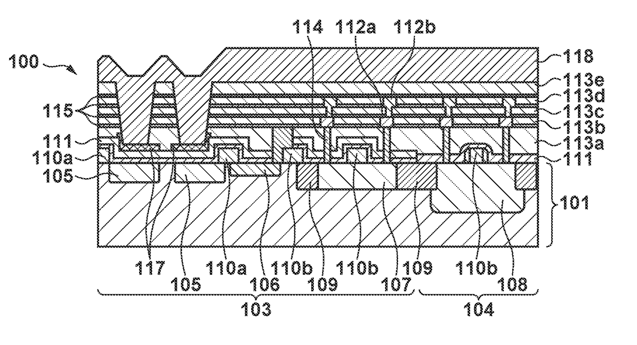
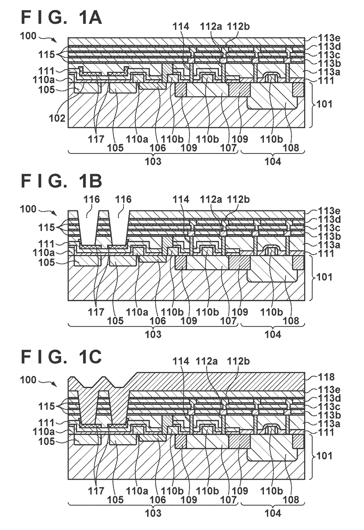
[0016]A method of manufacturing a solid-state image sensor according to the first embodiment of the present invention will be described with reference to the accompanying drawings. FIGS. 1A to 4C are schematic views of the sectional structure of a solid-state image sensor in the steps according to this embodiment. In each step, the solid-state image sensor halfway through the manufacture will also be referred to as a solid-state image sensor 100.

[0017]First, a semiconductor substrate 101 of the solid-state image sensor 100 is prepared. The semiconductor substrate 101 is a semiconductor material portion of members that constitute the solid-state image sensor 100. For example, the semiconductor substrate 101 includes a semiconductor wafer in which a semiconductor region is formed by a known semiconductor manufacturing process. An example of the semiconductor material is silicon. The interface between the semiconductor material and another material is a principal surfac...

Example

Second Embodiment

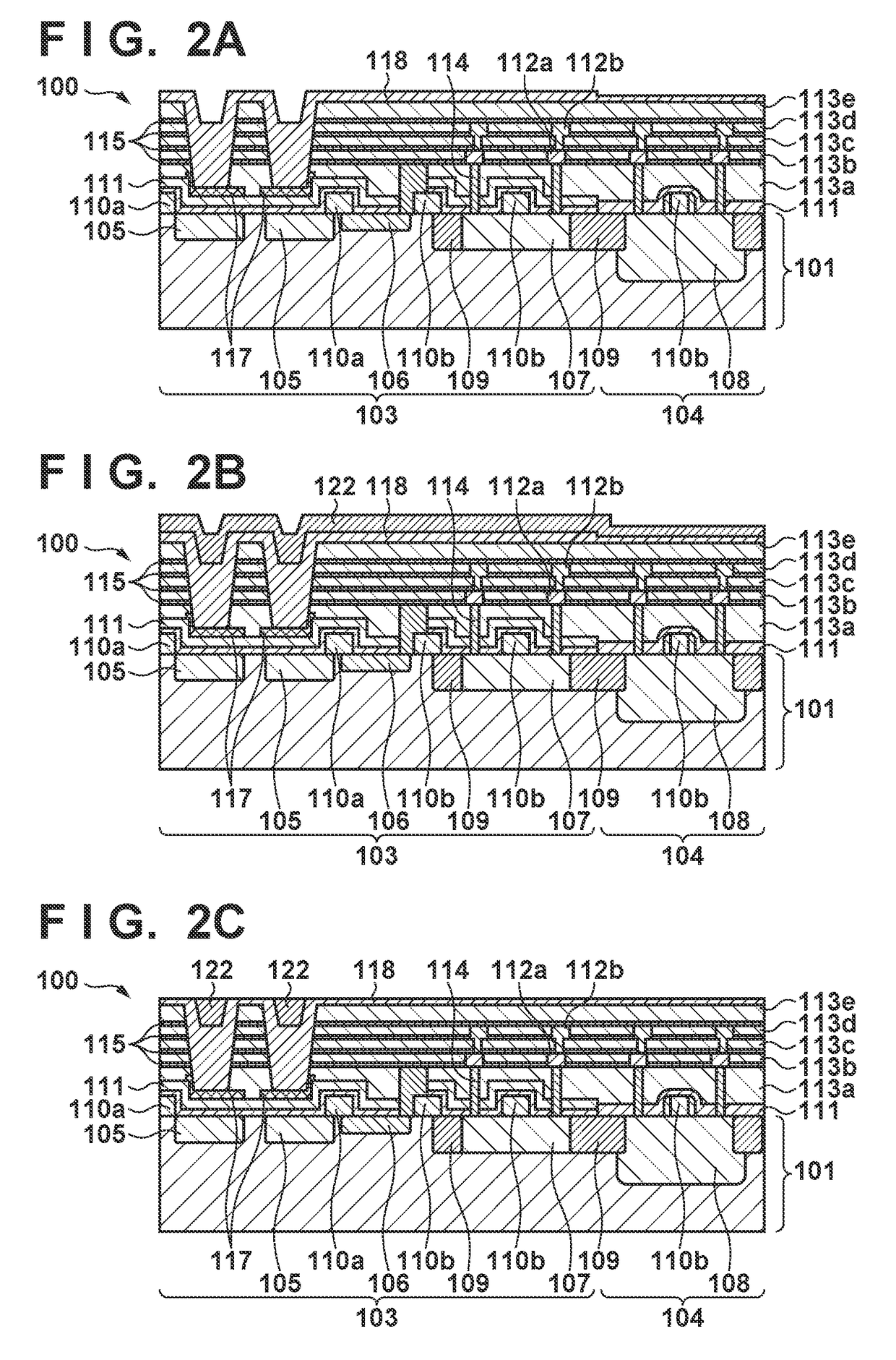
[0071]A method of manufacturing a solid-state image sensor according to the second embodiment of the present invention will be described with reference to FIGS. 6A to 7C. The same reference numerals as in FIGS. 1A to 5 denote parts having the same functions in FIGS. 6A to 7C, and a detailed description thereof will be omitted. An insulating member, which is formed from the first waveguide member 118, the second waveguide member 122, and the low refractive index member 123 in the first embodiment, is formed from only the first waveguide member 118 in the second embodiment.

[0072]FIG. 6A shows the same step as that shown in FIG. 1C of the first embodiment. That is, FIG. 6A shows a state in which the first waveguide member 118 is formed on a plurality of interlayer dielectric films 113a to 113e in which openings 116 are formed. The steps up to FIG. 6A in the method of this embodiment are the same as the steps shown in FIGS. 1A to 1C of the first embodiment.

[0073]In the ...


PUM


Abstract

A method of manufacturing a solid-state image sensor is provided. A first insulating member and an electrically conductive member is formed above a semiconductor substrate. A connecting portion of an upper surface of the electrically conductive member is covered with part of the first insulating member. First openings corresponding to the photoelectric conversion units are formed in the first insulating member. A second insulating member covering the first insulating member is then formed. The second insulating member is partially removed to expose the part of the first insulating member covering the connecting portion. A third insulating member that covers the first and second insulating members is then formed. The third insulating member is partially removed to expose the second insulating member. A second opening to expose the connecting portion is then formed to form a plug.

Description

BACKGROUND OF THE INVENTIONField of the Invention[0001]The present invention relates to a method of manufacturing a solid-state image sensor.Description of the Related Art[0002]There is proposed a solid-state image sensor including a light waveguide to increase the amount of light entering a photoelectric conversion unit. In Japanese Patent Laid-Open Nos. 2012-164945 and 2014-036036, an opening is formed in an insulating member of a low refractive index, and an insulating member of a high refractive index is formed on this insulating member. A portion of the insulating member of the high refractive index arranged in the opening forms the core of a light waveguide. The insulating member of the high refractive index is formed not only on the pixel region but also on the peripheral region. If the insulating member of the high refractive index remains when forming a plug in the peripheral region, it is difficult to form a through hole used to arrange the plug. Hence, in Japanese Patent ...

Claims


Application Information

Patent Timeline
IPC IPC(8): H01L27/146
CPCH01L27/14685H01L27/14645H01L27/14636H01L27/1463H01L27/14625H01L27/14627H01L31/18H01L27/14623H01L27/14609H01L27/14643H01L27/14612H01L31/0232H01L27/1462H01L27/14621
Inventor KANESADA, TAKAYASU
Owner CANON KK
Why Eureka
Try Eureka