Method to manufacture trench-first copper interconnection

Active Publication Date: 2013-08-27
SHANGHAI HUALI MICROELECTRONICS CORP
10 Cites 6 Cited by

AI-Extracted Technical Summary

Problems solved by technology

The double patterning technique needs two times of lithography and etch processes,...

Benefits of technology

[0016]The beneficial effects of the present invention are: forming metal interconnection by forming metal trench and VIA hole structures in the photoresist which can form a mask, via exposure and development through a lithography process, and then etching the metal trench and the VIA ho...

Abstract

The present invention relates to manufacturing technology of damascene copper interconnection in the semiconductor manufacturing field, and especially relates to a method to manufacture by trench-first copper interconnection. The method to manufacture trench-first copper interconnection forms metal trench and VIA hole structures in the photoresist which can form a hard mask through exposure and development processes, and then forms metal interconnection lines via etching metal trench and VIA hole in one etch process. The above method replaces the existing.

Application Domain

Technology Topic

Image

  • Method to manufacture trench-first copper interconnection
  • Method to manufacture trench-first copper interconnection
  • Method to manufacture trench-first copper interconnection

Examples

  • Experimental program(1)

Example

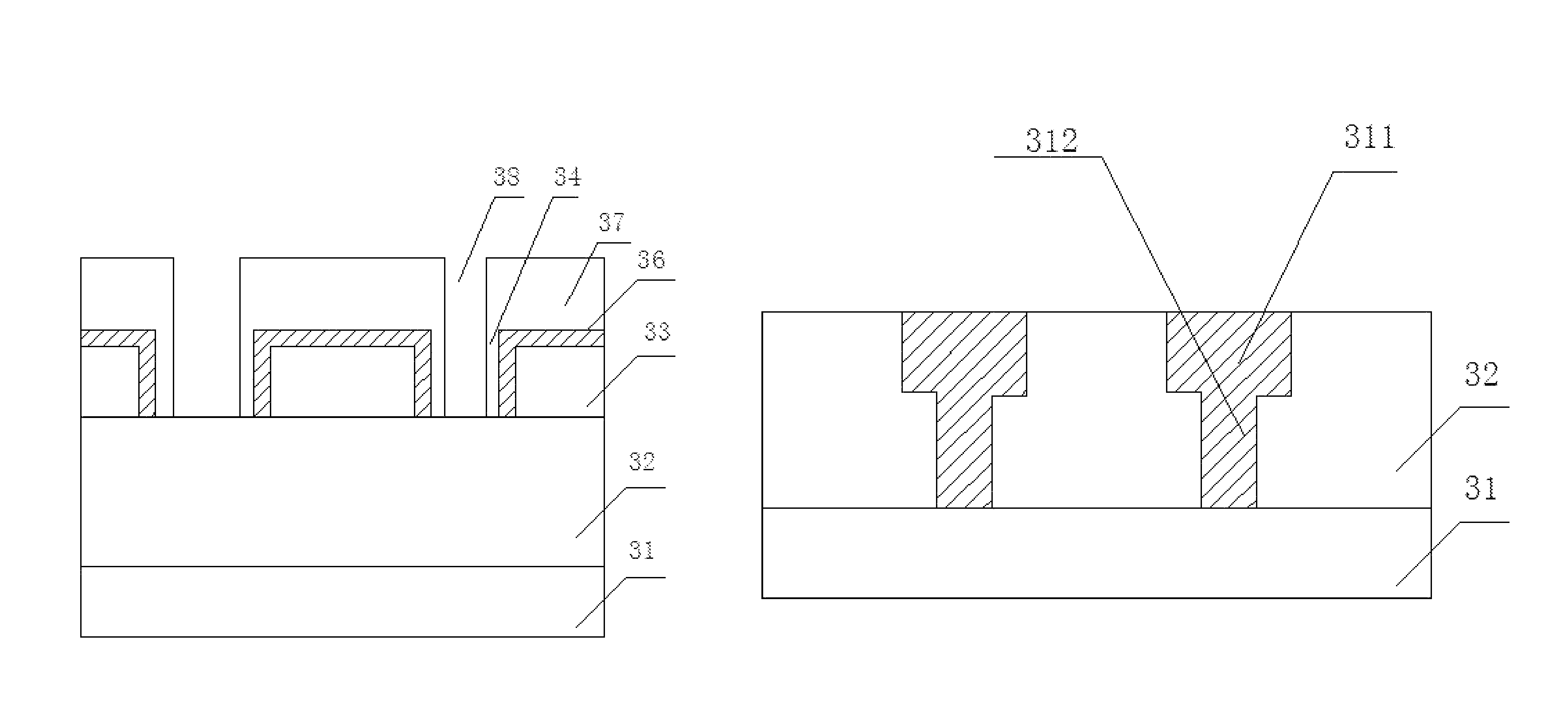
[0020]The following is a further description of the present invention combined with figs and embodiments.
[0021]As is shown in FIG. 3a-3i, a method to manufacture trench-first copper interconnection includes the following steps:
[0022]As is shown in FIG. 3a, in the step S1: firstly, depositing a dielectric layer 32 on a silicon substrate 31;
[0023]In an embodiment of this invention, the dielectric layer 32 is a low-k dielectric layer.
[0024]As is shown in FIG. 3b, in the step S2: coating a first photoresist 33 on the dielectric layer 32;
[0025]In this step, the first photoresist 33 is photoresist which can form hard mask, such as photoresist containing silyl group, siloxyl group, and silsesquioxane.
[0026]As is shown in FIG. 3c, in the step S3: after exposure and development through a lithography process, removing the first photoresist 33 until a portion of the upper surface of the dielectric layer 32 is exposed, and forming a first metal trench structure 34 in the rest first photoresist 33;
[0027]As is shown in FIG. 3d, in the step S4: coating curing material 35 to cover the upper surface of the first photoresist 33, the bottom and the side-wall of the first metal trench structure 34;
[0028]In this step, the curing material 35 is polymer material containing alkoxy group, such as acrylate or methacrylate polymer material containing alkoxy group.
[0029]As is shown in FIG. 3e, in the step S5: heating the curing material 35, and forming a separation film 36 on the upper surface of the rest first photoresist 33 after removing the redundant curing material 35;
[0030]In one embodiment of this invention, the range of the heating temperature comes from 30° C. to 200° C., and can prefer to be 50° C. to 170° C.;
[0031]In this step, removing the rest curing material 35 by developer.
[0032]As is shown in 3f, in the step S6: coating a second photoresist 37 to cover the upper surface of the separation film 36 and to fulfill the first metal trench structure 34 after the curing process, and then;
[0033]In this step, the ratio of the etching resistance of the first photoresist 33 and the second photoresist 37 is greater than or equal to 1.5:1, and said separation film 36 does not dissolve in the second photoresist 37.
[0034]As is shown in FIG. 3g, in the step S7: after exposure and development through a lithography process, removing the second photoresist 37 until a portion of the upper surface of the dielectric layer is exposed in the first metal trench structure, and forming a first VIA-hole structure 38 in the rest second photoresist 37 which is above the first metal trench structure 34;
[0035]As is shown in FIG. 3h, in the step S8: etching the dielectric layer 32 until a portion of the upper surface of the silicon substrate 31 using the rest second photoresist as a hard mask, and then removing the rest second photoresist 37 to form a second VIA hole 310; after removing the separation film, keep on etching a part of the rest dielectric layer 32 using the rest first photoresist as a hard mask, and then forming the second metal trench 39 after removing the rest first photoresist 33;
[0036]As is shown in FIG. 3i, in the step S9: filling metal material into the second VIA hole 310 and the second metal trench 39, to form VIA-hole interconnection structure 312 disposed in the second VIA hole and metal interconnection line 311 disposed in the second metal trench;
[0037]In this step, filling metal material into the second VIA hole 310 and the second metal trench 39 using metal deposition and CMP technology, to form VIA-hole interconnection structure 312 disposed in the second VIA hole and metal interconnection line 311 disposed in the second metal trench.
[0038]Although the above is a description in detail for embodiments of the present invention, the invention is not limited to those described embodiments, and the above embodiments are just examples. For the skilled in the art, any equivalent modifications and replacements are in the scope of the invention. Hence, equivalent modifications and replacements within the spirit and the range of the invention can be protected in the range of the invention.

PUM

no PUM

Description & Claims & Application Information

We can also present the details of the Description, Claims and Application information to help users get a comprehensive understanding of the technical details of the patent, such as background art, summary of invention, brief description of drawings, description of embodiments, and other original content. On the other hand, users can also determine the specific scope of protection of the technology through the list of claims; as well as understand the changes in the life cycle of the technology with the presentation of the patent timeline. Login to view more.

Similar technology patents

Cerium sulfate chelated sulfur dioxide, a preparation method and a use thereof

ActiveUS20190185336A1Step be reduceAvoid appearanceRare earth metal sulfatesChemical analysis using titrationSolventSulfur dioxide
Owner:SOUTH CHINA NORMAL UNIVERSITY

Classification and recommendation of technical efficacy words

  • Improve capacity
  • Step be reduce

Intelligent computer cabling

InactiveUS20060081716A1Step be reduceEliminates complexityProgram controlRecord carriers used with machinesEmbedded systemTransfer system
Owner:DATA DRIVE THRU

Dual-chamber syringe and associated connecting systems

InactiveUS20160175537A1Step be reduceImprove techniqueInfusion syringesCheck valvesQuality assuranceSyringe
Owner:THORNE CONSULTING FOR INT PROPERTY LLC
Why Eureka
Try Eureka