Method for fabricating semiconductor device

Inactive Publication Date: 2006-06-29
SK HYNIX INC
View PDF8 Cites 0 Cited by
  • Summary
  • Abstract
  • Description
  • Claims
  • Application Information

AI Technical Summary

Benefits of technology

[0019] It is, therefore, an object of the present invention to provide a method for fabricating a semiconductor device which reduces proc

Problems solved by technology

Accordingly, a channel length has been more reduced, thereby providing a lot of limitations.
At this time, the reason for performing the process of patterning the anti-reflective coating layer 12 and the photoresist layer 13, and the process of recessing the substrate region X in two separate chambers is because if the both processes are performed in one chamber, other problems may arise.
First, if the above two processes are performed in the same chamber for patterning the oxide layer, the device isolation layers 11 made of the HDP oxide layer may be excessively etched.
At this time, there is a high possibility that a height difference caused by damage in the device isolation layers 11 due to the cleaning process generates remnants of polysilicon for a gate or a change in an effective fOX height (EFH), thereby inducing defects in semiconductor memory devices.
Accordingly, th

Method used


Image

  • Method for fabricating semiconductor device
  • Method for fabricating semiconductor device
  • Method for fabricating semiconductor device

Examples


Example

[0025] Hereinafter, detailed descriptions on preferred embodiments of the present invention will be provided with reference to the accompanying drawings.

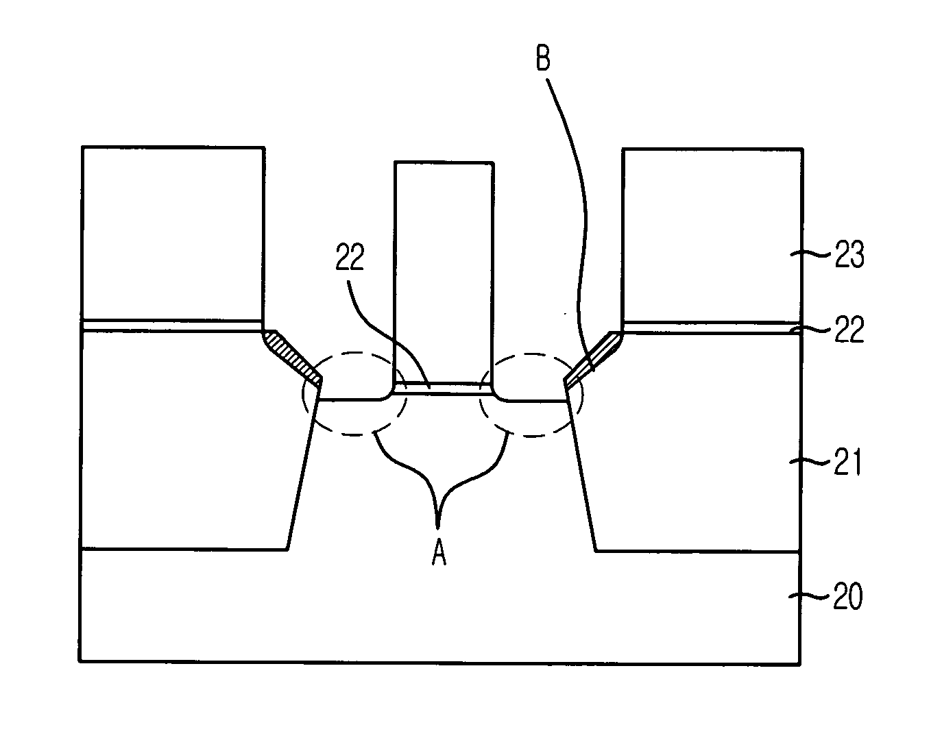
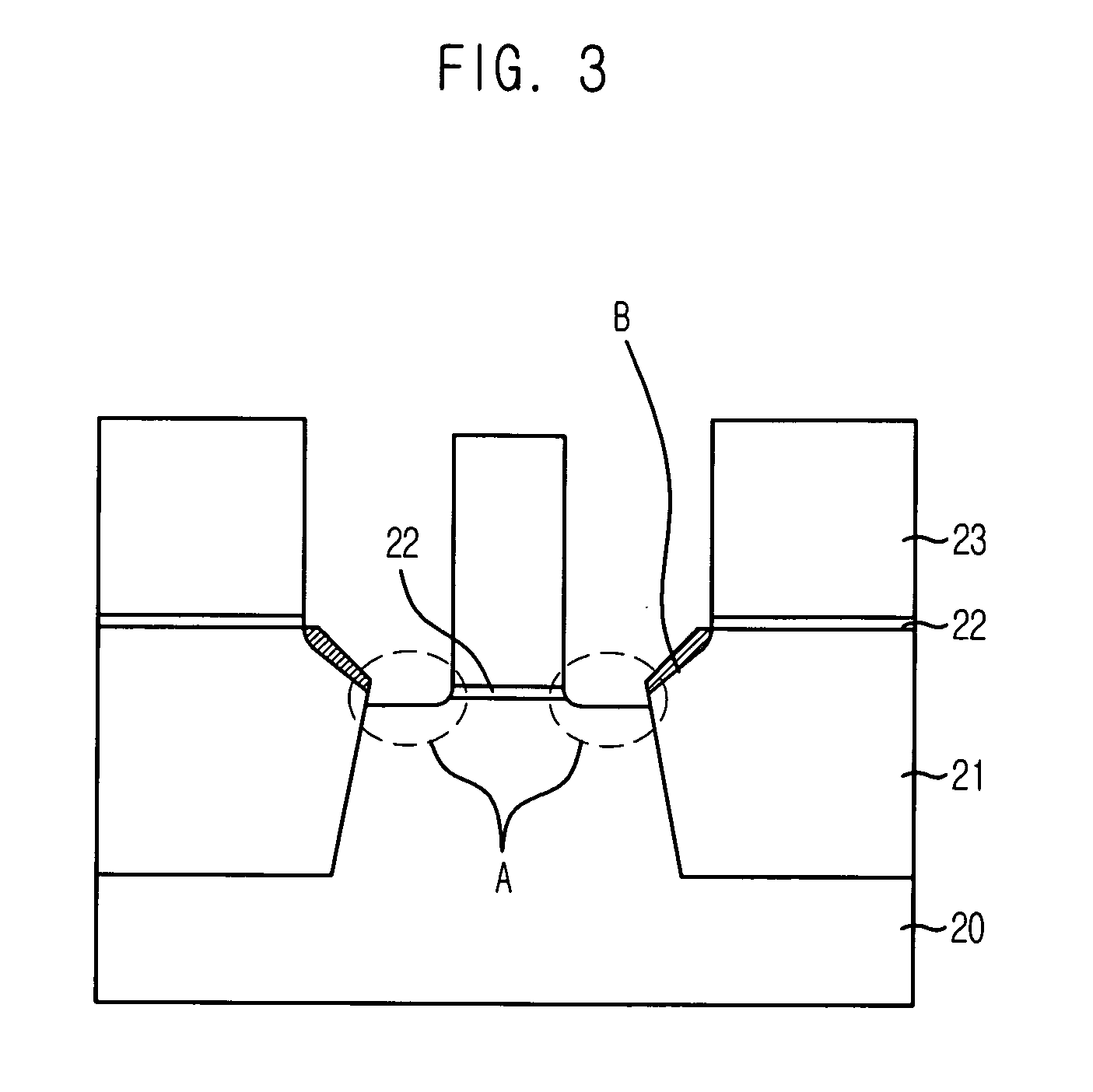
[0026]FIG. 3 is a cross-sectional view illustrating a method for fabricating a semiconductor device in accordance with a specific embodiment of the present invention. It should be noted that the same reference numerals are used for the same elements described in FIG. 2.

[0027] Referring to FIG. 3, first, a plurality of predetermined trench regions are formed on a substrate 20 and then, the trench regions are filled with an insulation layer, thereby forming shallow trench isolation (STI) type device isolation layers 21. The device isolation layers 21 include an oxide layer using high density plasma (HDP).

[0028] An anti-reflective coating layer 22 and a photoresist layer 23 are deposited on an entire surface of the substrate 20.

[0029] In a chamber used for patterning an oxide layer, the anti-reflective coating layer 22 and the phot...


PUM


Abstract

A method for fabricating a semiconductor device is provided. The method includes: forming device isolation layers on a substrate; sequentially forming an anti-reflective coating layer and a photoresist layer on the substrate; patterning the anti-reflective coating layer and the photoresist layer to expose substrate regions in which active regions of a metal oxide semiconductor (MOS) transistor will be formed; and recessing the exposed substrate regions in a predetermined thickness.

Description

FIELD OF THE INVENTION [0001] The present invention relates to a method for fabricating a semiconductor device; and more particularly, to a method for fabricating a semiconductor device capable of effectively expanding a channel of a metal-oxide-semiconductor (MOS) transistor. DESCRIPTION OF RELATED ARTS [0002] A first process to form semiconductor circuits on a substrate is a process of forming a device isolation layer which isolates devices from each other. [0003] Initially, the device isolation layer was formed through a local oxidation of silicon (LOCOS) method; however, as the integration scale of semiconductor devices has been increased, the device isolation layer has been formed through a shallow trench isolation (STI) method more advantageous on the integration. [0004] Meanwhile, as the semiconductor devices have been highly integrated, a design rule of MOS transistors has been reduced and thus, a gate pattern size has been also reduced. Accordingly, a channel length has bee...

Claims


Application Information

Patent Timeline
IPC IPC(8): H01L21/461
CPCH01L21/3065H01L29/66636H01L21/18
Inventor NAM, KI-WONKIM, JAE-YOUNG
Owner SK HYNIX INC
Why Eureka
Try Eureka