Supercharge Your Innovation With Domain-Expert AI Agents!

Manufacturing method of a circuit board having a glass film

Active Publication Date: 2018-01-04
UNIMICRON TECH CORP
View PDF3 Cites 2 Cited by
  • Summary
  • Abstract
  • Description
  • Claims
  • Application Information

AI Technical Summary

Benefits of technology

The invention provides a solution for improving the reliability and yield of circuit board structures by avoiding the problem of warping. This is achieved by using a thinner glass film on the electrostatic chuck, which is laser-etched to form conductive vias. A circuit layer is then formed on the glass film, and the electrostatic chuck is removed. By doing so, a redistribution layer structure can be completed without the need for de-bonding, which reduces stress and prevents warping.

Problems solved by technology

However, when the glass substrate is de-bonded, it is easy to cause the problem of warping resulted from the stress issue since the material of the dielectric layer is too soft.
The problem of warping may reduce reliability and yield of the product.

Method used


Image

  • Manufacturing method of a circuit board having a glass film
  • Manufacturing method of a circuit board having a glass film
  • Manufacturing method of a circuit board having a glass film

Examples


first embodiment

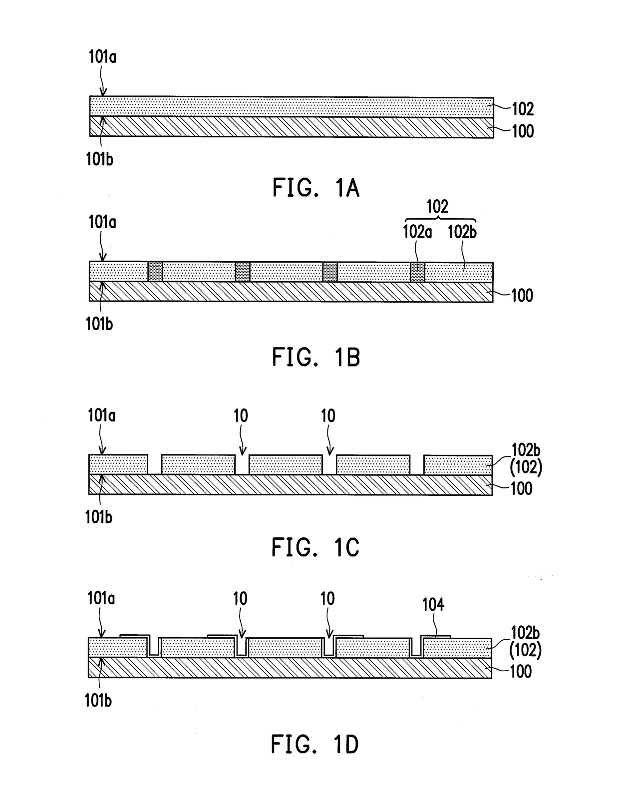
[0021]FIG. 1A to FIG. 1H are schematic cross-sectional diagrams of a manufacturing process of a circuit board structure according to the invention.

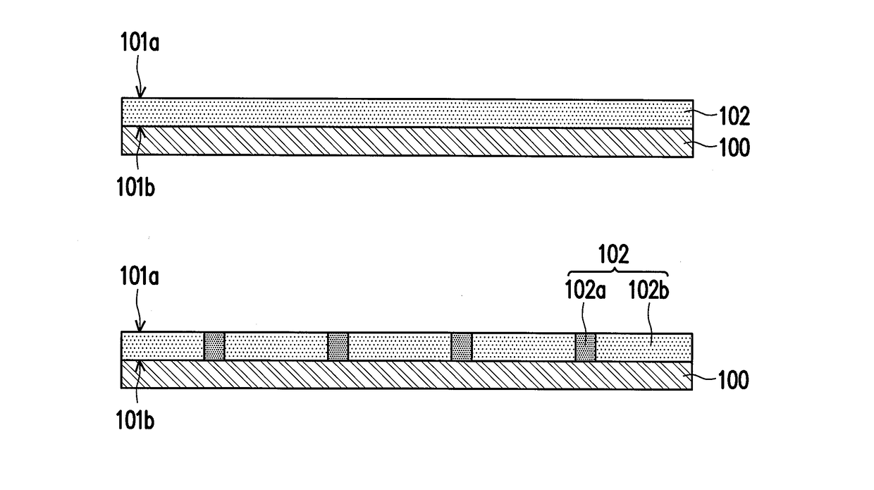
[0022]Referring to FIG. 1A, a glass film 102 is provided on an electrostatic chuck 100, wherein the glass film 102 has an upper surface 101a and a lower surface 101b opposite to each other. In particular, the electrostatic chuck 100 can absorb the lower surface 101b of the glass film 102 by electrostatic force, such that the glass film 102 is held on the electrostatic chuck 100 without warping. In an embodiment, a thickness of the glass film 102 may be between 5 micrometers and 100 micrometers, for example. Preferably, the thickness of the glass film may be 10 micrometers, 20 micrometers, 30 micrometers, 50 micrometers, or 80 micrometers, for example. A size of the glass film 102 may be adjusted according to the needs of a user.

[0023]Referring to FIG. 1B, a laser light is irradiated to the glass film 102, so as to form a plurality of modi...

second embodiment

[0032]FIG. 2A to FIG. 2D are schematic cross-sectional diagrams of a manufacturing process of a circuit board structure according to the invention.

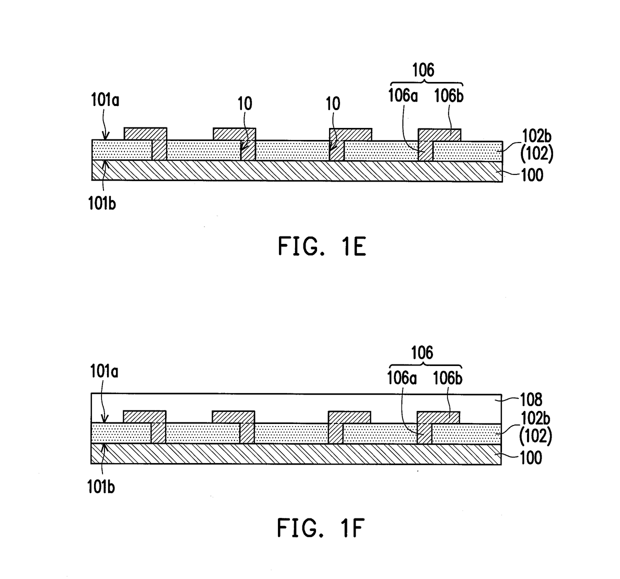
[0033]Referring to FIG. 1H and FIG. 2A, the first circuit board structure 1 of FIG. 1H is flipped on the electrostatic chuck 100, such that the lower surface 101b of the glass film 102 is upward. Thereafter, the first circuit board structure 1 is absorbed by electrostatic force (more particularly, the first circuit board structure 1 is absorbed on the second circuit layer 110b), such that the first circuit board structure 1 is held on the electrostatic chuck 100 without warping.

[0034]Referring to FIG. 2A and FIG. 2B, a third circuit layer 206 is formed on the lower surface 101b of the glass film 102, such that the third circuit layer 206 is electrically connected with the first conductive vias 106a. A material and a forming method of the third circuit layer 206 is similar to the material and the forming method of the first circuit layer 1...


PUM

PropertyMeasurementUnit
Thicknessaaaaaaaaaa
Thicknessaaaaaaaaaa
Electrical conductoraaaaaaaaaa

Abstract

Provided is a manufacturing method of a circuit board structure including steps as below. A glass film is provided on an electrostatic chuck (E-chuck). A plurality of first conductive vias are formed in the glass film. A first circuit layer is formed on an upper surface of the glass film, such that the first circuit layer is electrically connected with the first conductive vias. A first polymer layer is formed on the first circuit layer. The first polymer layer covers a surface of the first circuit layer and the upper surface of the glass film. A plurality of second conductive vias are formed in the first polymer layer. A second circuit layer is formed on the first polymer layer, such that the second circuit layer is electrically connected with the second conductive vias. The E-chuck is removed.

Description

BACKGROUND OF THE INVENTIONField of the Invention[0001]The invention relates to a semiconductor structure and a manufacturing method thereof, and particularly relates to a circuit board structure and a manufacturing method thereof.Description of Related Art[0002]Since the requirements for portability and multi-function of consumer electronics products are increased, a semiconductor device is moving towards a trend of small size, high performance, and low cost. In this trend, the semiconductor device is required to add more input / output (I / O) pads onto a circuit board in a smaller area. In other words, with a higher integrity of the semiconductor device, the requirements for reliability and yield of semiconductor packaging technology is higher.[0003]A glass substrate is often used as a carrier in a conventional circuit board process, and a multilayer circuit layer and a multilayer dielectric layer are formed on the glass substrate respectively. Then, the glass substrate is de-bonded,...

Claims


Application Information

Patent Timeline
IPC IPC(8): H01L23/498H05K3/12H05K1/11H01L21/48H05K1/03H01L21/683H05K3/40H05K3/00
CPCH01L23/49838Y10T29/49165H05K1/0306H05K3/0029H05K1/115H05K3/1275H05K3/0023H05K3/4038H01L21/4857H01L21/486H01L23/49822H01L23/49827H05K3/002H01L21/4853H05K3/4007H01L21/6833H05K3/188H05K3/424H05K3/4605H05K2201/09136H05K2201/09536H05K2201/09563H05K2203/0165H05K2203/107H05K2203/1563
Inventor WULI, CHIEN-TSAILO, CHENG-CHUNG
Owner UNIMICRON TECH CORP
Features
  • R&D
  • Intellectual Property
  • Life Sciences
  • Materials
  • Tech Scout
  • Unparalleled Data Quality
  • Higher Quality Content
  • 60% Fewer Hallucinations
Learn More