Goa driving circuit

a driving circuit and circuit technology, applied in the field of display technology, can solve the problems of poor stability and circuit failure risk, and achieve the effect of promoting the stability of the goa driving circuit and reducing the failure risk

Active Publication Date: 2018-02-15
WUHAN CHINA STAR OPTOELECTRONICS TECH CO LTD
View PDF0 Cites 14 Cited by
  • Summary
  • Abstract
  • Description
  • Claims
  • Application Information

AI Technical Summary

Benefits of technology

[0061]The benefits of the present invention are: the present invention provides a GOA driving circuit. In the screen awakening stage, the first global control signal controls the twelfth thin film transistors in the GOA units of all stage to be activated for realizing the All Gate On function. The first global control signal controls the eleventh thin film transistors in the GOA units of all stage to be activated to pull down the voltage levels of the second nodes for ensuring the normal output of the output ends; in the reset stage, the reset signal controls the first thin film transistor to reset the voltage level of the second node, and to set the duration of the single pulse of the reset signal to be at least the sum of durations of initial pulses of the first clock signal and the second clock signal for ensuring that the second node is at high voltage level after the screen is awakened so that the output of the GOA driving circuit can be normal, and the touch display panel enters normal display after the screen is awakened; in the touch scan stage, the second global control signal controls the thirteenth thin film transistors in the GOA units of all stage to be activated to make the output ends of the GOA units of the respective stages output composite signals. In this stage, the composite signal is a pulse signal having the same frequency with the touch scan signal for ensuring that the touch scan is normally performed. Accordingly, the GOA driving circuit of the present invention can ensure that the touch display panel performs normal display after the screen is awakened to eliminate the failure risk as the GOA circuit achieves the All Gate On and touch scan function for promoting the stability of the GOA driving circuit.

Problems solved by technology

However, the circuit failure risk exist as the GOA circuit applied in the touch display panel according to prior art achieves the All Gate On and the touch scan function, and the stability is worse.

Method used


Image

  • Goa driving circuit
  • Goa driving circuit
  • Goa driving circuit

Examples


first embodiment

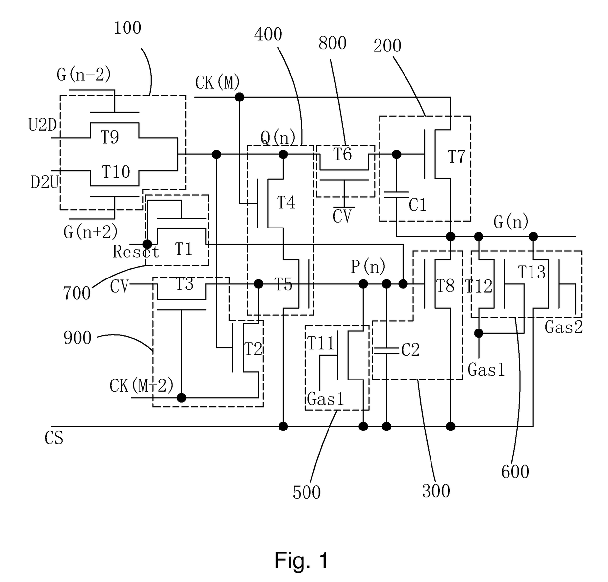
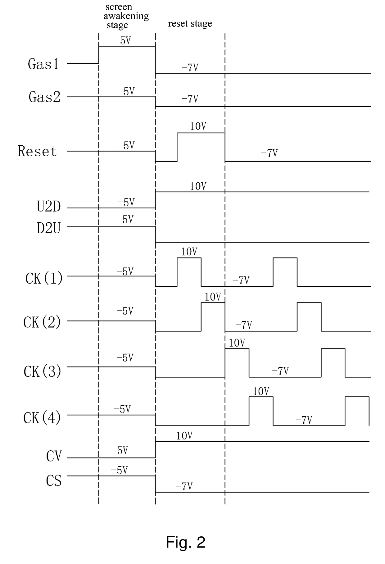
[0088]Please refer to FIG. 1, FIG. 2 and FIG. 3 at the same time, or refer to FIG. 1, FIG. 2 and FIG. 4 at the same time. For the first embodiment according to the GOA driving circuit of the present invention, the respective thin film transistors are all N-type thin film transistors; in the screen awakening stage, the first global control signal Gas1 is high voltage level, and the second global control signal Gas2 is low voltage level; in the reset stage and the normal display stage, both the first global control signal Gas1 and the second global control signal Gas2 are low voltage levels; in the touch scan stage, the second global control signal Gas2 is high voltage level, and the first global control signal Gas1 is low voltage level. Significantly, in the reset stage, that a duration of the single pulse of the reset signal is at least a sum of durations of initial pulses of a first clock signal CK(1) and a second clock signal CK(2) means that the single pulse of the reset signal R...

second embodiment

[0091]Please refer to FIG. 9. For the second embodiment according to the GOA driving circuit of the present invention, the respective thin film transistors are all P-type thin film transistors; and then, in the screen awakening stage, the first global control signal Gas1 is low voltage level, and the second global control signal Gas2 is high voltage level; in the reset stage and the normal display stage, both the first global control signal Gas1 and the second global control signal Gas2 are high voltage levels; in the touch scan stage, the second global control signal Gas2 is low voltage level, and the first global control signal Gas1 is high voltage level.

[0092]In the reset stage and the normal display stage, a voltage level of the composite signal CS is high voltage level, and the control voltage level CV is low voltage level; all the respective clock signals are periodic high voltage level pulse signals. Selectably, in the touch scan stage, all voltage levels of the respective cl...


PUM


Abstract

Disclosed is a GOA driving circuit. In screen awakening stage, the first global control signal (Gas1) controls the twelfth thin film transistor (T12) to be activated for realizing the All Gate On function, and meanwhile controls the eleventh thin film transistor (T11) to be activated to pull down the voltage level of the second node (P(n)); in reset stage, the reset signal (Reset) controls the first thin film transistor (T1) to reset the voltage level of the second node (P(n)), and to set the duration of the single pulse of the reset signal (Reset) to be at least the sum of durations of initial pulses of the first, second clock signals; in touch scan stage, the second global control signal (Gas2) controls the thirteenth thin film transistor (T13) to be activated to make the output ends of the GOA units of the respective stages output composite signals (CS).

Description

FIELD OF THE INVENTION[0001]The present invention relates to a display technology field, and more particularly to a GOA driving circuit.BACKGROUND OF THE INVENTION[0002]The Liquid Crystal Display (LCD) possesses advantages of thin body, power saving and no radiation to be widely used in many application scope, such as LCD TV, mobile phone, personal digital assistant (PDA), digital camera, notebook, laptop, and dominates the flat panel display field.[0003]The Active Matrix Liquid Crystal Display (AMLCD) is the most common liquid crystal display device at present. The Active Matrix Liquid Crystal Display comprises a plurality of pixels, and each pixel comprises a Thin Film Transistor (TFT). The gate of the TFT is coupled to the scan line extending along the horizontal direction. The drain of the TFT is coupled to the data line extending along the vertical direction. The source of the TFT is coupled to the corresponding pixel electrode. When a sufficient positive voltage is applied to ...

Claims


Application Information

Patent Timeline
Patent Type & Authority Applications(United States)
IPC IPC(8): G06F3/041G09G3/36
CPCG09G2310/0286G11C19/28G06F3/0416G09G3/3659G09G3/3677G09G2354/00G09G2310/08G09G2300/0871G09G2310/0245G09G2310/063G09G2310/0281G09G2310/0289G09G2310/021G09G2300/0852G06F3/0412G09G3/20G09G2300/0408G09G2310/0283G06F3/04166G09G3/36
Inventor XIAO, JUNCHENGYAN, YAOCAO, SHANGCAODAI, RONGLEI
Owner WUHAN CHINA STAR OPTOELECTRONICS TECH CO LTD
Why Eureka
Try Eureka