Semiconductor device and scan test method

a technology of a semiconductor device and a scan test, which is applied in the direction of measurement devices, error detection/correction, instruments, etc., can solve the problems of inability to take out correct test results stably, inability to supply correct test data, and difficulty in timing design in some cases, so as to reduce the occurrence of timing violations and shorten the execution time

Active Publication Date: 2018-03-01
RENESAS ELECTRONICS CORP
View PDF1 Cites 16 Cited by
  • Summary
  • Abstract
  • Description
  • Claims
  • Application Information

AI Technical Summary

Benefits of technology

[0016]According to one embodiment described above, it is possible to perform a scan test with the reduced occurrence of timing violations and in a shorter execution time.

Problems solved by technology

When supply of test data to a plurality of scan chains does not satisfy the above condition, it is not possible to supply correct test data to all flip-flops and thereby not possible to take out correct test results stably.
However, in a runtime test mechanism that includes a circuit which performs the above-described scan test, timing design is difficult in some cases.
An example of the case where timing design is difficult is when STA (Static Timing Analysis) cannot be carried out (it is virtually impossible due to too complicated conditions) in the case where a CPU (Central Processing Unit) core is located in a DVFS (Dynamic Voltage and Frequency Scaling) region (region where the voltage and frequency vary) and a circuit for controlling a runtime test is located in a CONST region (region where the voltage and frequency do not vary).
However, this results in a failure to satisfy requirements (e.g., completion of a runtime test in 10 msec) related to a runtime test execution time (FTTI: fault tolerant time interval).
However, in the techniques disclosed in Patent Literature 1 and Patent Literature 2, setup time violations cannot be avoided while hold-time violations can be avoided.
There is thus a problem that it is not possible to perform a scan test without the occurrence of timing violations.
However, in the technique disclosed in Patent Literature 3, a scan test can be performed only after all the scan-in data are loaded at a low-rate scan clock, and therefore it has a problem that the time needed for a scan test increases.

Method used


Image

  • Semiconductor device and scan test method
  • Semiconductor device and scan test method
  • Semiconductor device and scan test method

Examples


first embodiment

[Overall Configuration]

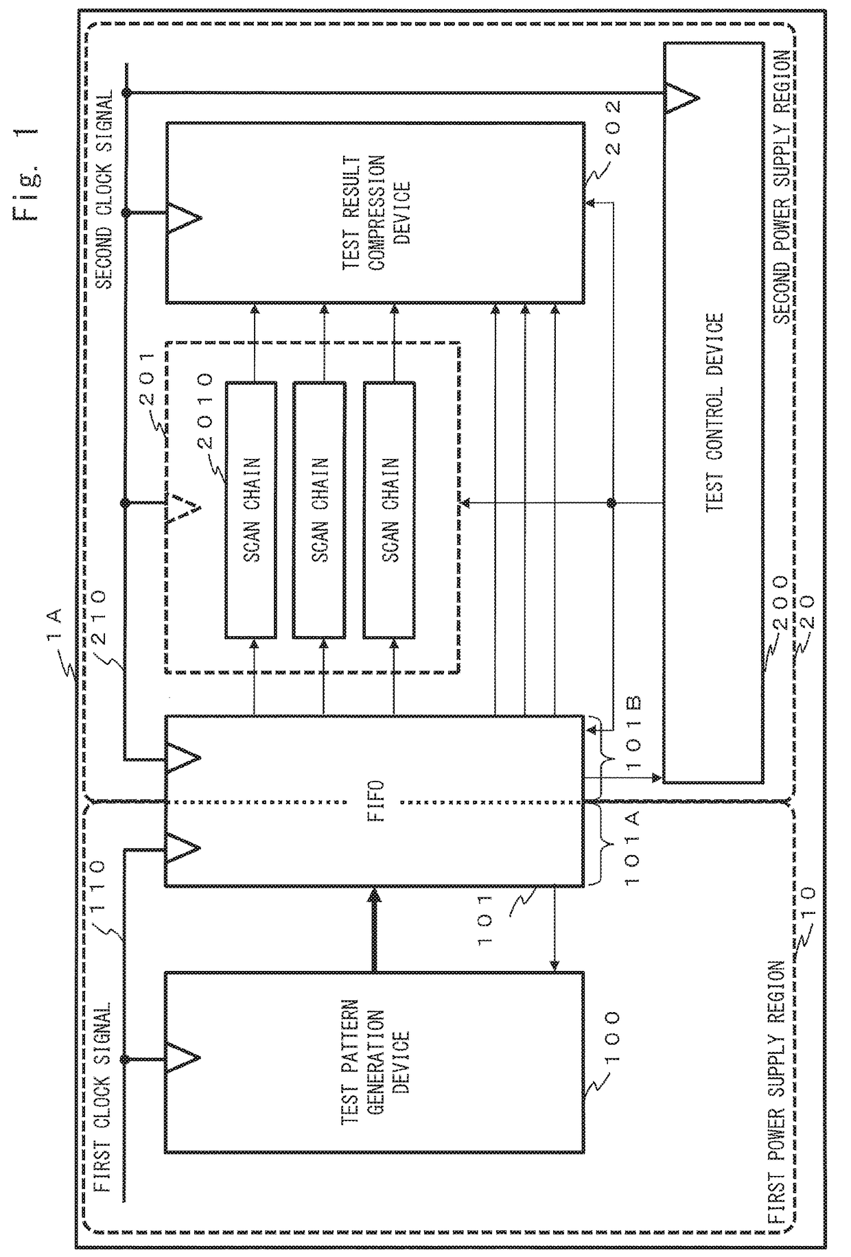
[0038]The configuration of a semiconductor device (1A) according to the first embodiment is described hereinafter with reference to FIG. 1. FIG. 1 is a block diagram of the semiconductor device (1A) according to the first embodiment.

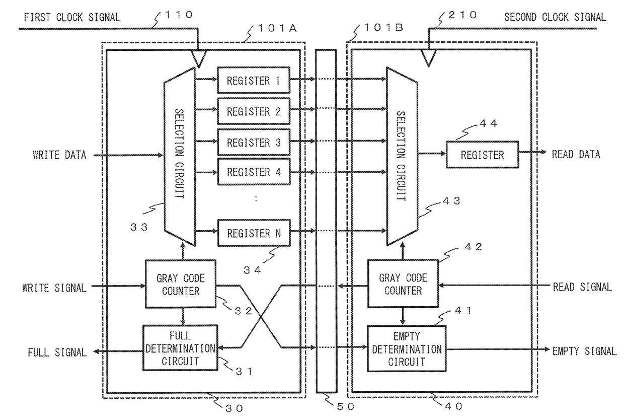
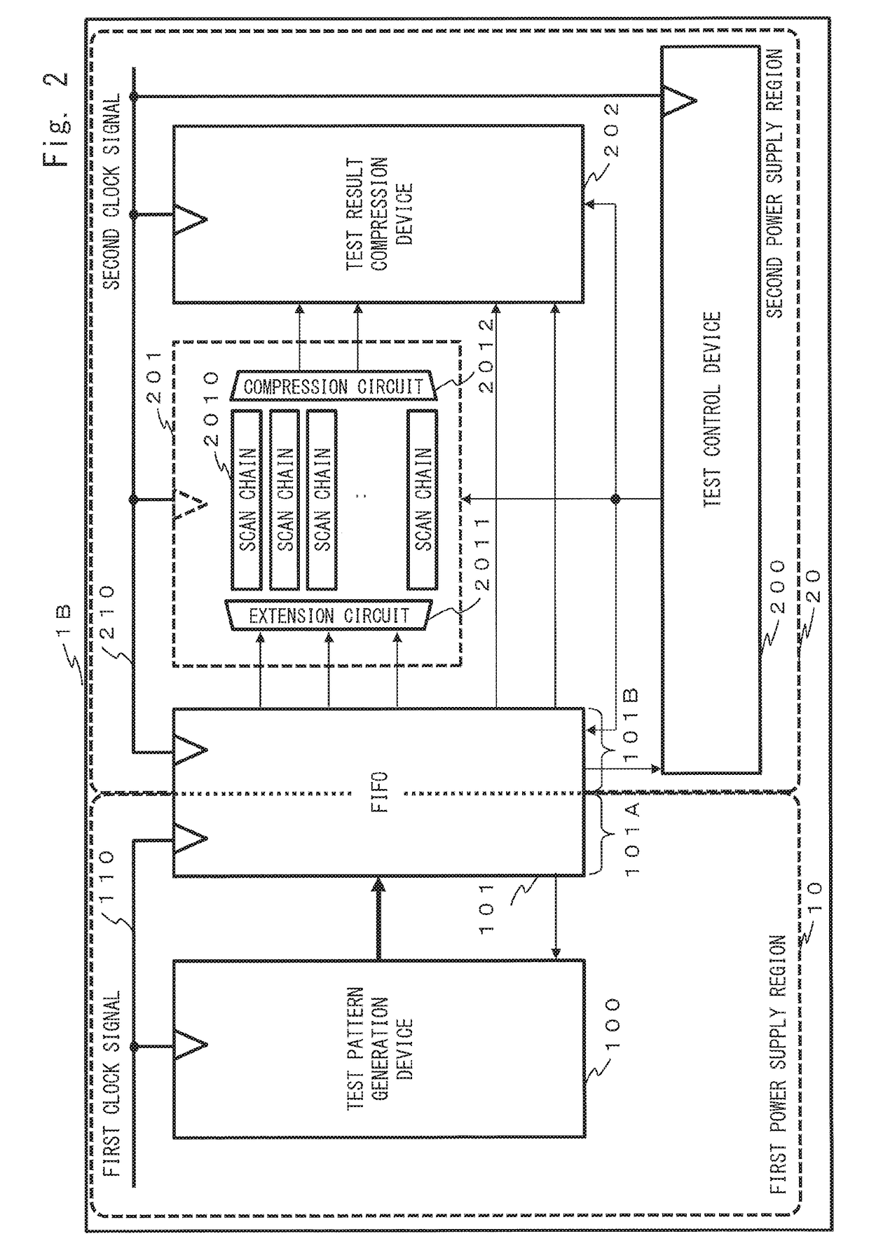
[0039]As shown in FIG. 1, the semiconductor device (1A) includes a test pattern generation device (100), a FIFO (101), a test control device (200), a circuit to be tested (201), and a test result compression device (202). The semiconductor device (1A) includes a first power supply region (10) and a second power supply region (20), and power supply lines are different between the first power supply region (10) and the second power supply region (20).

[0040]A first power supply region (10) includes the test pattern generation device (100). A second power supply region (20) includes the test control device (200), the circuit to be tested (201), and the test result compression device (202). Some functional block (101A) in the FIFO (101)...

second embodiment

[0131]A second embodiment is described hereinbelow. In the following description of the second embodiment, the same elements as in the first embodiment described above are denoted by the same reference symbols or the like, and the description of the same is omitted as appropriate.

[Overall Configuration]

[0132]The configuration of a semiconductor device (1C) according to the second embodiment is described hereinafter with reference to FIG. 7. FIG. 7 is a schematic diagram of the semiconductor device (1C) according to the second embodiment.

[0133]As shown in FIG. 7, the semiconductor device (1C) according to the second embodiment is different from the semiconductor device (1B) according to the first embodiment in that it further includes a test clock control device (203).

[0134]The test clock control device (203) is included in the second power supply region (20). The second clock signal (210) is input to the test clock control device (203). Thus, the test clock control device (203) is d...

third embodiment

[0164]A third embodiment is described hereinbelow. In the following description of the third embodiment, the same elements as in the second embodiment described above are denoted by the same reference symbols or the like, and the description of the same is omitted as appropriate.

[Overall Configuration]

[0165]The configuration of a semiconductor device (1D) according to the third embodiment is described hereinafter with reference to FIG. 11. FIG. 11 is a schematic diagram of the semiconductor device (1D) according to the third embodiment. The semiconductor device (1D) according to the third embodiment is an embodiment that is suitable for execution of a runtime test with use of a scan test mechanism.

[0166]As shown in FIG. 11, the semiconductor device (1D) according to the third embodiment is different from the semiconductor device (1C) according to the second embodiment in that it includes a test pattern read device (102) instead of the test pattern generation device (100), and furthe...


PUM


Abstract

A semiconductor device includes a FIFO, a test data write circuit that sequentially writes a plurality of test data to the FIFO in synchronization with a first clock signal, and a test control circuit that, in parallel with writing of the plurality of test data to the FIFO by the test data write circuit, sequentially reads a plurality of test data stored in the FIFO in synchronization with a second clock signal that is not synchronous with the first clock signal and performs a scan test of a circuit to be tested.

Description

TECHNICAL FIELD[0001]The present invention relates to a semiconductor device and a scan test method and, particularly, relates to a semiconductor device including circuits that operate in synchronization with different clock signals.TECHNICAL FIELD[0002]A scan test is typically used as a test of a semiconductor device. A semiconductor device capable of performing a scan test has a scan chain, which is a shift register. The shift register is constructed by connecting flip-flops that forma logic. A scan test is performed by inputting test data to a flip-flop in the first stage of the scan chain.[0003]In general, the scan chain is split into a plurality of segments in order to reduce the time needed for a scan test. Each of the scan chains has an input for taking test data in and an output for taking test results out. Test results are sequentially taken out of the flip-flop in the final stage of the scan chain and checked against an expected value, and thereby the test results of the s...

Claims


Application Information

Patent Timeline
Patent Type & Authority Applications(United States)
IPC IPC(8): G01R31/319G01R31/3185G01R31/3193G06F11/267
CPCG01R31/31921G01R31/318516G01R31/3193G01R31/318594G01R31/318508G06F11/267G01R31/318547G01R31/318572G01R31/318536G01R31/31922
Inventor MAEDA, YOICHIMATSUSHIMA, JUNWADA, HIROKI
Owner RENESAS ELECTRONICS CORP
Why Eureka
Try Eureka