Textured surfaces for display applications

a technology of textured surfaces and display applications, applied in the direction of diffusing elements, mechanical instruments, instruments, etc., can solve the problems of affecting the appearance of the display, the contrast ratio of the display is greatly limited, and the performance characteristics of the transparent display are susceptible to several poor performance characteristics, etc., to achieve the effect of not particularly limited substrate size and high light transmission

Active Publication Date: 2018-03-01
CORNING INC
View PDF1 Cites 6 Cited by
  • Summary
  • Abstract
  • Description
  • Claims
  • Application Information

AI Technical Summary

Benefits of technology

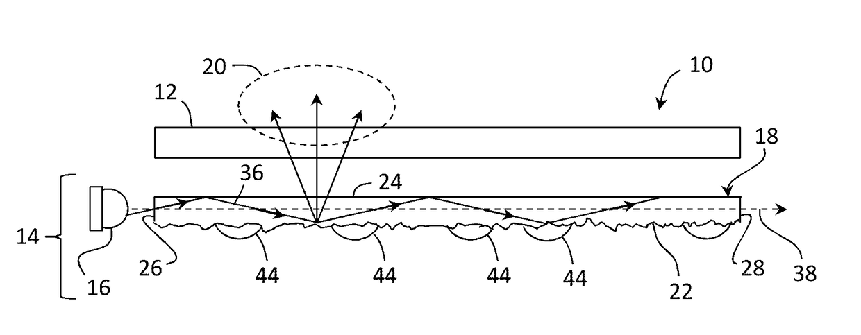
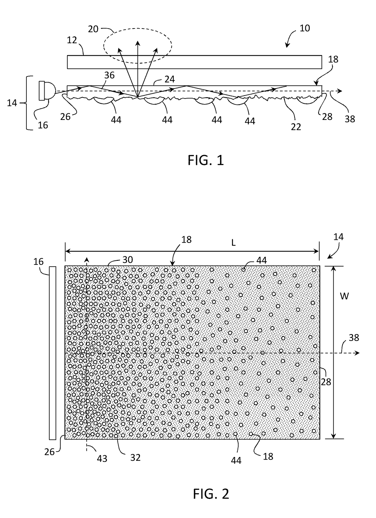
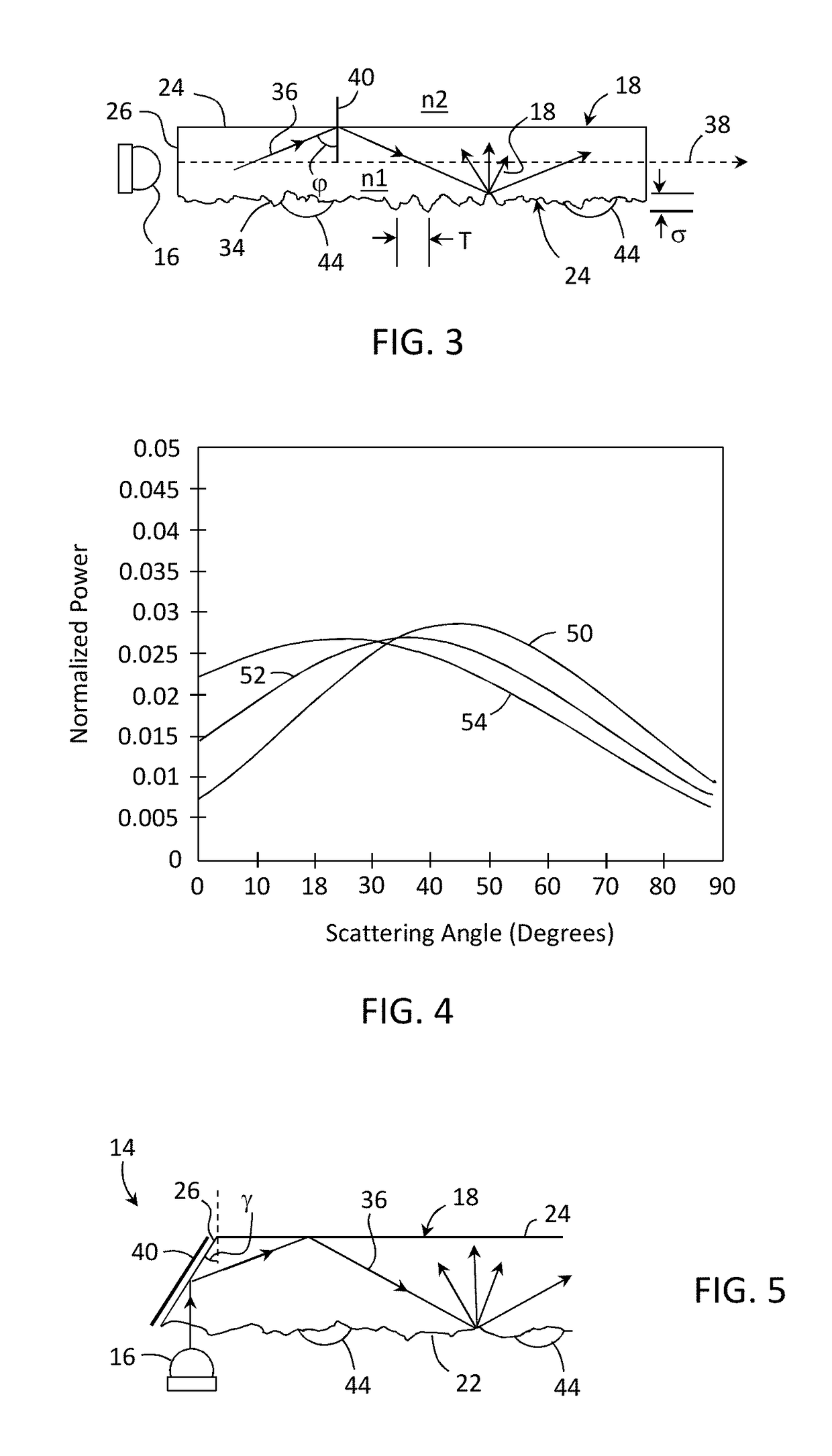
[0010]Thus, in accordance with one or more embodiments presented herein, a light emitter is described. As used herein, the term light emitter refers generically to a device configured to provide illumination. The light emitter may, for example, include a back light element for use in a display device, or the light emitter may be configured to provide general illumination such as illumination for a room or vehicle. The light emitter includes a light guide into which light can be coupled by one or more slight sources and through which the coupled light propagates. The light guide is generally a substrate comprising opposing major surfaces. As used herein, the term substrate refers generally to a plate-like substrate and which in some embodiments is suitable for use as a light guide. The substrate may be planar, or the substrate may, in some examples, have a wedge-like shape. Nevertheless, the substrate generally has two opposing major surfaces bounded by edge surfaces. The major surfaces may be planar and parallel, or the major surfaces may be planar and non-parallel. In some embodiments the substrate may be curved, for example as used in a curved display device. For light emitter applications at least one of the opposing major surfaces includes a surface texture configured to scatter at least a portion of the light propagating within the light guide. The surface texture is specifically configured to render the light guide visually transparent, without appreciable haze, thereby making the light guide particularly useful in the construction of a back light element for use in a transparent display device. The configuration of the surface texture also provides excellent viewing angle performance.
[0040]In still another embodiment a method of forming a light guide is described comprising treating a surface of a glass substrate with an etchant comprising acetic acid, for example glacial acetic acid, in an amount from about 92% to about 98% by weight, ammonium fluoride in an amount from about 0.5% to about 5.5% by weight, and less than 6% by weight water. While not wishing to be bound by any particular theory, it is believed that for some embodiments the lower the water content, the lower the ammonium fluoride dissociation rate, which leads to a reduced release of HF. A reduced concentration of HF can also lead to a reduction in the removal of glass from the glass substrate, which in turn results in shallower pits in the etched surface thereof, which is needed for low haze (e.g. greater transparency). Additionally, reduced water content can provide for a reduction in the solubility of the precipitated crystal mask in the etchant. This means the mask stays on the glass substrate surface longer. When the nucleated crystals stay undissolved on the glass surface, the etch rate for the etchant is lower and the crystal lateral dimension remains unchanged, thus leading to the desired low correlation length.

Problems solved by technology

Unfortunately, transparent displays are susceptible to several poor performance characteristics.
In actuality, currently available displays only partially transmit and reflect light, thus the contrast ratio of the display is greatly limited.
Commercially available transparent displays typically offer only about 15% transmission, and performance is even lower in reflection mode.
Back lights having a frosted appearance are generally unacceptable.
Existing technology for providing backplane illumination are not satisfactorily meeting certain cost and performance requirements of the marketplace for transparent displays.
Other components of display devices, particularly the substrates forming the display panel itself, may present problems during manufacture of the thin film devices formed on at least one of the substrates.
For example, triboelectrification can impede the ability to remove the substrate from surfaces in contact with the substrate, which can lead to breakage of the substrate and particle generation in some cases.
This can be particularly troublesome for substrates, such as glass substrates, produced via processes that result in extremely smooth surfaces on the substrate.
To maintain the semi-transparent characteristics, these conventional display systems do not employ an opaque optical light emitter to produce light.
As discussed above, a significant issue with current “transparent” display systems is that they are not particularly transparent.
Thus, a relatively high level of ambient light may be needed in proximity to the display panel, which might not always be feasible or even desirable for any number of reasons.
The result is an array of problems related to uniformity of image quality across the display, such as non-uniformity in color, contrast ratio, etc.
The range of such designed patterns is limited only by the designer's imagination.
Ordinarily, such an image projected onto a transparent substrate, for example a glass plate not configured to scatter light, will not be readily visible at the transparent substrate.
Instead, light rays from the projection system will be substantially transmitted through the substrate making it difficult if not impossible to view the projected image on the substrate.

Method used


Image

  • Textured surfaces for display applications
  • Textured surfaces for display applications
  • Textured surfaces for display applications

Examples


example 1

[0184]Corning® Code 2320 glass samples were etched in solutions 1-6 from Table 1. Brightness and haze were measured and the data are presented below in Table 2. Code 2320 glass is a sodium alumino silicate glass.

TABLE 2Decayexponent,Brightness @ 3 mm,SampleSolutionmm−1, bWatts% Haze110.0122.96E−070.791111220.0092.57E−070.346667330.0123.03E−070.715556440.0134.09E−070.798889550.0124.75E−070.856667660.0216.39E−074.261111

[0185]As the data show, samples exposed to etchants 1-5 are similar in respect of the attenuation of light. A good metric to compare brightness uniformity of the two conditions is b, the exponent in an exponential fit (e.g., where the fit equation is of the form y=Aebx) of the brightness data. The data of Table 2 describe a brightness decay exponent b ranging from about 0.009 mm−1 to about 0.013 mm−1 and with etchant 2 exhibiting the lowest brightness decay. The sample treated with etchant 6, although initially brighter than the others, exhibited a steeper decay curve w...

example 2

[0195]In a series of experiments, 0.7 mm thick Corning code 2318 glass samples having dimensions of 150 mm×150 mm were etched by immersing the samples in a mixture of glacial acetic acid and aqueous ammonium fluoride. Corning code 2318 is an alkali alumino silicate glass. The samples were etched in a bath with a component ratio of 15:6:4 of glacial acetic acid, water and ammonium fluoride, respectively. The etchant bath immersion time was 3 minutes, after which the samples were rinsed in de-ionized water and air dried. The samples were lighted along one edge surface using an LED strip and the brightness of the samples' output at a major surface thereof was measured starting from the edge nearest the LED strip across to the opposite edge.

[0196]The etched surfaces of the samples were then printed with a transparent resin in selected areas using a FujiFilm® Dimatix™ 2831 ink jet printer with a 1 picoLiter print head, depositing droplets of resin, each resin droplet containing approxima...

example 3

[0199]In one laboratory experiment glass substrate samples were cooled in a freezer to a temperature of about −19° C.) and a refrigerator to a temperature of about −4° C., heated to various temperatures in an oven, then immediately etched in a fresh solution #2 (as shown in Table 1), and rinsed. Glass temperature experiments were performed on two separate dates approximately 1 week apart, and strong positive log correlations (R2>0.95) were exhibited between glass temperature prior to etch and the VAG parameter, as seen in FIG. 22. However, this relationship was not the same from one day to the next. It is believed that changes in the relative humidity, room temperature and dew point between the two dates may have been responsible for differences in the glass temperature vs. VAG curves shown, and stabilizing the etching environments could eliminate this variability.


PUM

PropertyMeasurementUnit
RMS roughnessaaaaaaaaaa
wavelengthaaaaaaaaaa

Abstract

A substrate with a textured surface is disclosed. The substrate may be, for example, a light emitter comprising a light guide, for example a backlight element for use in a display device, wherein a surface of the light guide, for example a glass substrate, is configured to have a textured surface with a predetermined RMS roughness and a predetermined correlation length of the texture. A plurality of light scatter suppressing features can be provided on the textured surface. Textured surfaces disclosed herein may be effective to reduce electrostatic charging of the substrate surface. Methods of producing the textured surface are also disclosed.

Description

CROSS-REFERENCE TO RELATED APPLICATIONS[0001]This application is a divisional of U.S. patent application Ser. No. 15 / 105,025 filed Jun. 16, 2016 which claims the benefit of priority under 35 U.S.C. §371 of International Patent Application Serial No. PCT / US14 / 70771, filed Dec. 17, 2014, which claims the benefit of priority under 35 U.S.C. §119 of U.S. Provisional Application Ser. No. 61 / 918,276 filed on Dec. 19, 2013, the content of which is relied upon and incorporated herein by reference in their entiretyBACKGROUNDField[0002]The present invention relates generally to textured surfaces for display applications. For example, a textured surface as disclosed herein may be used in a light emitter (e.g., a backlight for certain display devices), the light emitter comprising a substrate with a textured surface on one or both major surfaces of the substrate that can operate as a light guide, and processes for making the light emitter. The light guide may include a pattern of discrete dots ...

Claims


Application Information

Patent Timeline
Patent Type & Authority Applications(United States)
IPC IPC(8): F21V8/00C03C15/00G02B5/02
CPCG02B6/0065G02B6/0061G02B6/0036G02B5/0294G02B6/0068G02B5/0221G02B1/118C03C15/00G02B5/0278C03C17/32C03C2218/119G02B1/111
Inventor NOLAN, DANIEL ALOYSIUSRAVICHANDRAN, VASUDHAROUDAS, IOANNIS GEORGIOSWOLCOTT, CHRISTINE COULTER
Owner CORNING INC
Why Eureka
Try Eureka