Light emitting device cooling

Active Publication Date: 2018-03-01
KONINKLJIJKE PHILIPS NV
View PDF5 Cites 4 Cited by
  • Summary
  • Abstract
  • Description
  • Claims
  • Application Information

AI Technical Summary

Benefits of technology

[0014]By directly connecting a metal heat transfer element between the sides of the chip and the board, heat dissipation is improved. This is in addition to the heat transfer between the electrical contacts to the light emitting layer and the contact pads on the board. Thus, there is an additional heat transfer path which allows for improved heat dissipation and hence a reduction in the temperature of the light emitting d

Problems solved by technology

The light output of light emitting diodes in modern light emitting devices is typically limited by temperature related behaviour.
Light emitting devices are often required to work for long periods of time without replacement.
In some cases, the light emitting devices are located at locations wher

Method used


Image

  • Light emitting device cooling
  • Light emitting device cooling
  • Light emitting device cooling

Examples


Example

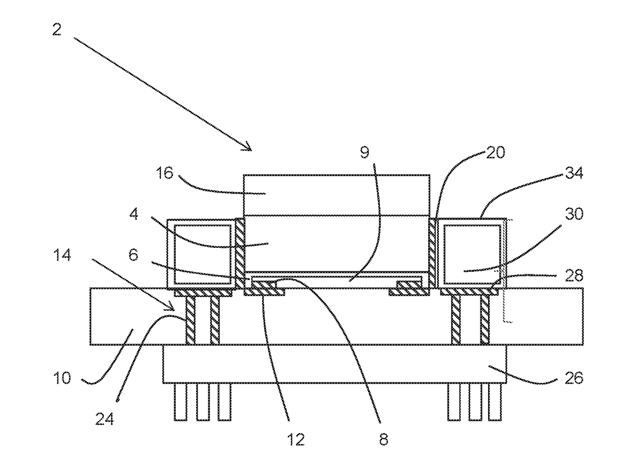
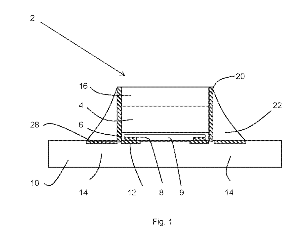
[0050]The invention provides a method of manufacturing a light emitting device and the resulting device.

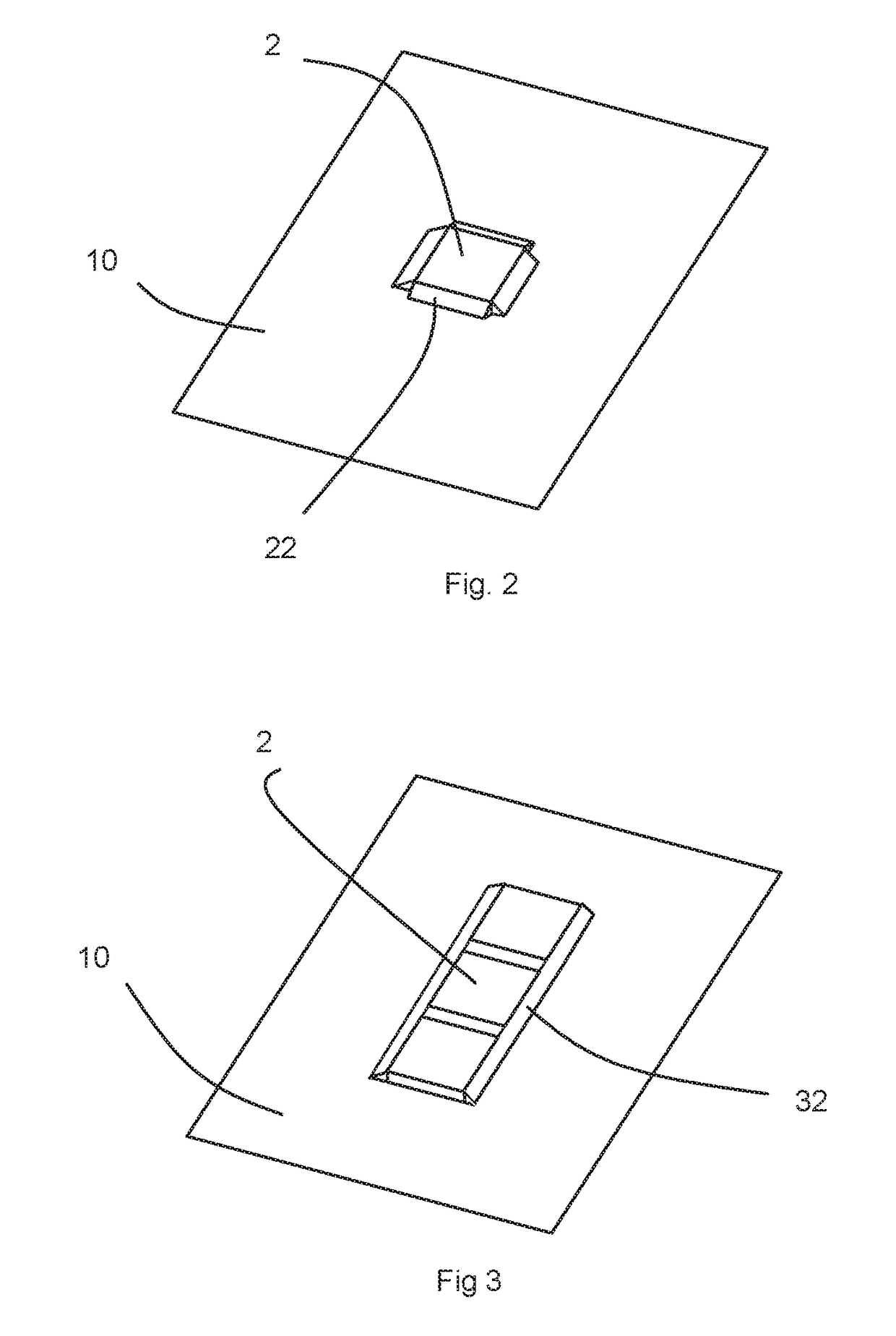
[0051]A light emitting device chip 2 according to an example has a sapphire substrate 4 and a light emitting semiconductor layer 6 on one face of the sapphire substrate 4. The light emitting semiconductor layer 6 is an epilayer on the sapphire substrate 4. Electrical contacts 8 are provided on a first major surface of the light emitting device chip directly connecting to the light emitting semiconductor layer. The light emitting semiconductor layer 6 comprises a light emitting diode which may be referred to generally as a light emitting region 9, and may have a number of sub-layers doped n and p type to emit light when an electric current is passed through, the current being introduced from electrical contacts 8. The light emitting diode 9 is electrically isolated from the edges of the light emitting semiconductor layer 6.

[0052]The light emitting device chip 2 is mounted on board ...


PUM


Abstract

A light emitting device such as luminaire includes one or more light emitting device chips mounted on a board. The light emitting device chips have electrical contacts and are flip chip mounted to board with the electrical contacts connected to contact pads. Sidewall metallisations on the sidewalls of the light emitting device chips are connected by metal heat transfer elements to heat dissipation regions of board. The metal heat transfer elements may be of solder which may be deposited using equipment conventionally used for attaching surface mount devices.

Description

FIELD OF THE INVENTION[0001]The invention relates to a light emitting device and method of manufacture.BACKGROUND OF THE INVENTION[0002]Semiconductor light emitting devices are increasingly been used in a wide variety of applications. In a particular example, luminaires using a number of light emitting diodes to emit light are increasingly being used for lighting applications to replace technologies such as incandescent light bulbs or fluorescent lamps. By mounting a plurality of light emitting diodes on a substrate, a variety of different light outputs can be achieved.[0003]The light output of light emitting diodes in modern light emitting devices is typically limited by temperature related behaviour. One constraint on light output is provided by the thermo-electric behaviour of the semiconductor material of the light emitting diodes, for example thermal and current droop. In order to produce white light, a suitable phosphor is often used and the phosphor can quench at high tempera...

Claims


Application Information

Patent Timeline
IPC IPC(8): H01L33/64H01L33/62H01L33/50
CPCH01L33/644H01L33/62H01L33/505H01L33/642H01L2933/0066H01L2933/0075H01L25/0753F21K9/232F21Y2115/10F21V19/0015H01L33/44H01L33/64H01L33/486
Inventor SWEEGERS, NORBERTUS ANTONIUS MARIADE SAMBER, MARC ANDREZUIDEMA, PATRICK
Owner KONINKLJIJKE PHILIPS NV
Why Eureka
Try Eureka