Control circuit for semiconductor switching element, and semiconductor device

a control circuit and switching element technology, applied in the direction of spark gap circuits, instruments, pulse techniques, etc., can solve the problems of abnormally high temperature detection, and increasing the risk of causing an erroneous temperature detection. , to achieve the effect of preventing unnecessary overheating protection

Active Publication Date: 2018-03-01
MITSUBISHI ELECTRIC CORP
View PDF8 Cites 10 Cited by
  • Summary
  • Abstract
  • Description
  • Claims
  • Application Information

AI Technical Summary

Benefits of technology

[0017]According to the present invention, a determination as to whether or not overheat protection is necessary is made based on both an overheat detection signal and a current detection signal. Accordingly, it is possible to turn off the semiconductor switching element only when a certain amount of load current is flowing to the semiconductor switching element and the semiconductor switching element is determined to have reached an abnormal temperature. As a result, even if the overheat detection signal is output by mistake, an unnecessary overheat protection can be prevented from being performed.
[0018]FIG. 1 is a diagram illustrating an ignitor semiconductor device according to the first embodiment

Problems solved by technology

Thus, an abnormally high temperature can be detected.
When the L load noise (displacement current) 100 in association with the operation of the switching element 5 is ge

Method used


Image

  • Control circuit for semiconductor switching element, and semiconductor device
  • Control circuit for semiconductor switching element, and semiconductor device
  • Control circuit for semiconductor switching element, and semiconductor device

Examples


first embodiment

[Configuration of Device of First Embodiment]

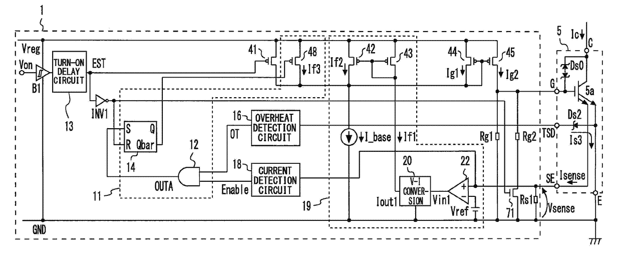
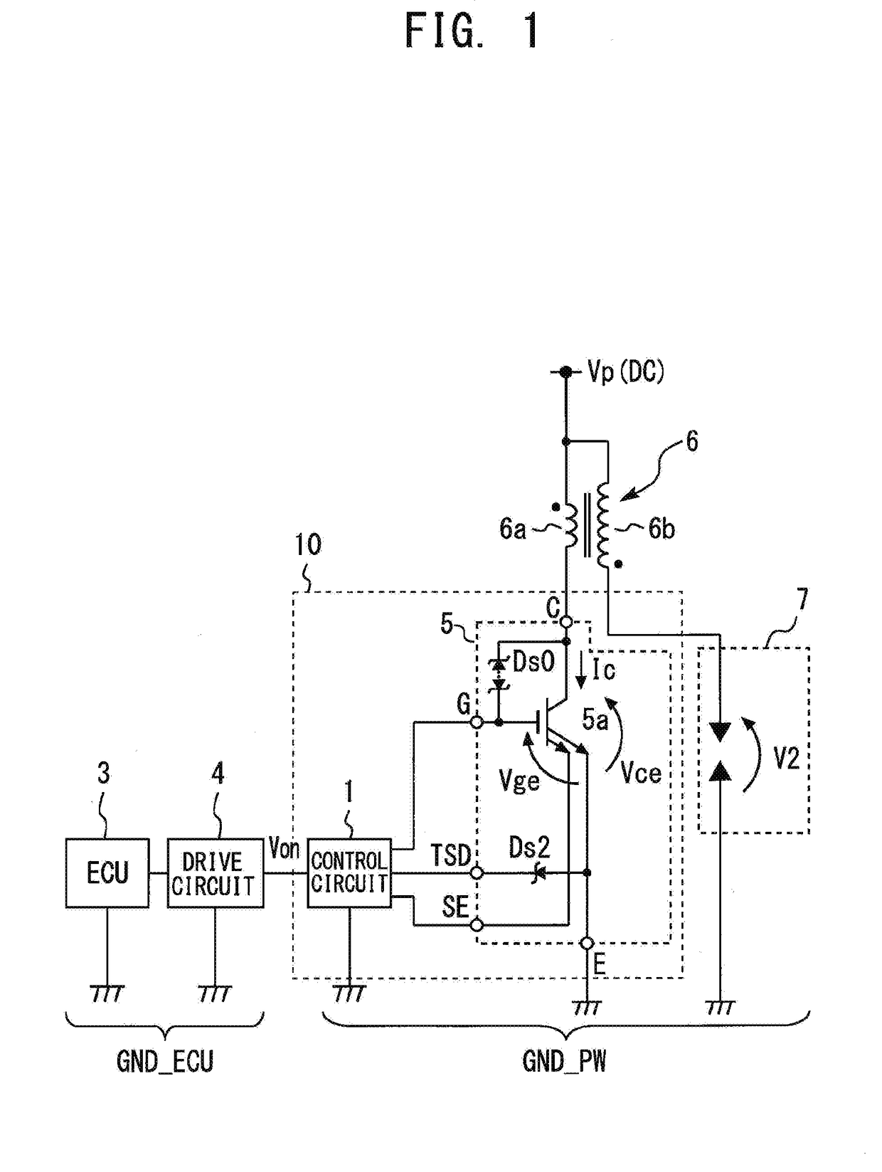
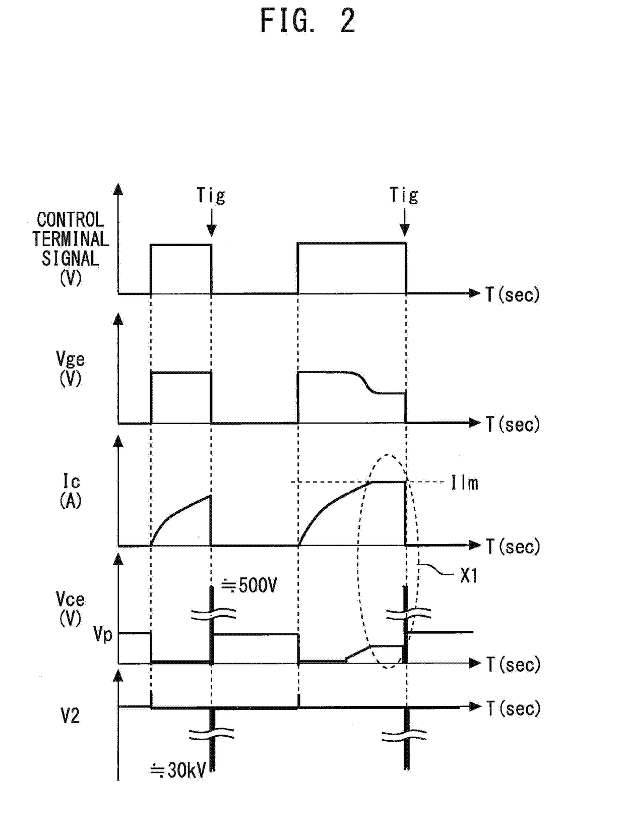
[0043]FIG. 1 is a diagram illustrating an ignitor semiconductor device 10 according to the first embodiment of the present invention. FIG. 2 is a timing diagram illustrating the operation of the ignitor semiconductor device 10 according to the first embodiment of the present invention. An ignition system (induced ignition system) for an internal combustion engine, such as a vehicle engine, as illustrated in FIG. 1, includes each component for generating a high voltage to be applied to a spark plug 7. Specifically, this ignition system includes a transformer 6 which is an ignition coil (induction load; hereinafter referred to also as “L load”), the semiconductor device 10, which is a so-called igniter for controlling a current caused to flow through the transformer 6, an electronic control unit (ECU) 3 for engine control including a computer, and a drive circuit 4 which is provided between the ECU 3 and a control circuit 1. The semiconduct...

second embodiment

[0097]An ignitor semiconductor device according to a second embodiment has a circuit configuration similar to that of the semiconductor device 10 according to the first embodiment, except that the control circuit 1 is replaced by a control circuit 201. The control circuit 201 according to the second embodiment has a circuit configuration similar to that of the control circuit 1 according to the first embodiment, except that an attenuating circuit 210 is added. Accordingly, in the following description, the same or corresponding components as those of the first embodiment are denoted by the same reference numerals, differences between the second embodiment and the first embodiment are mainly described and the descriptions of common features are abbreviated or omitted.

[0098]FIG. 9 is a diagram illustrating the control circuit 201 of the switching element according to the second embodiment of the present invention. The control circuit 201 according to the second embodiment includes the...

third embodiment

[0106]An ignitor semiconductor device according to the third embodiment has a circuit configuration similar to that of the ignitor semiconductor device 10 according to the first embodiment, except that the control circuit 1 is replaced by a control circuit 301. The control circuit 301 according to the third embodiment has a circuit configuration similar to that of the control circuit 1 according to the first embodiment, except that an attenuating circuit 310 is added. Accordingly, in the following description, the same or corresponding components as those of the first embodiment are denoted by the same reference numerals, differences between the third embodiment and the first embodiment are mainly described and the descriptions of common features are abbreviated or omitted.

[0107]FIG. 11 is a diagram illustrating the control circuit 301 of the switching element according to the third embodiment of the present invention. The attenuating circuit 310 has a circuit configuration similar ...


PUM


Abstract

A control circuit for a semiconductor switching element includes a control terminal, a main electrode terminal, and a current sensing terminal, and controls the semiconductor switching element including a diode connected to the main electrode terminal or the current sensing terminal. The control circuit includes an overheat detection circuit, a current detection circuit, and an interruption circuit. The overheat detection circuit outputs an overheat detection signal when a temperature detected based on an output of the diode is equal to or higher than a predetermined set temperature. The current detection circuit outputs a current detection signal when an output value of the current sensing terminal is equal to or greater than a predetermined set current value. The interruption circuit turns off the semiconductor switching element when both the overheat detection signal from the overheat detection circuit and the current detection signal from the current detection circuit are input.

Description

FIELD[0001]The present invention relates to a control circuit for a semiconductor switching element, and a semiconductor device.BACKGROUND[0002]For example, as disclosed in JP 2011-124269 A, an ignitor semiconductor device for controlling a semiconductor switching element to be turned on or off to ignite a spark plug of an internal combustion engine is conventionally known. In the device disclosed in JP 2011-124269 A, the temperature of the semiconductor switching element is detected using a current signal obtained through a diode by utilizing temperature characteristic of the diode, which is used for overheat protection.CITATION LISTPatent Literature[0003][PTL 1] JP 2011-124269 A[0004][PTL 2] WO 2012 / 077187SUMMARYTechnical Problem[0005]An ignition system for an internal combustion engine, such as a vehicle engine, includes an ignition coil (induction load; hereinafter referred to also as “L load”) for generating a high voltage to be applied to the spark plug. When the temperature o...

Claims


Application Information

Patent Timeline
IPC IPC(8): H02M1/08F02P3/04G05F1/56H01T15/00
CPCH02M1/08F02P3/0435G05F1/561H01T15/00F02P3/053F02P3/0554H03K17/0828H03K2017/0806H03K2217/0027F02P3/055
Inventor YAMAMOTO, KOJIKAWAMOTO, ATSUNOBUGODO, SHINSUKE
Owner MITSUBISHI ELECTRIC CORP
Why Eureka
Try Eureka