Chip package structure and manufacturing method thereof

Active Publication Date: 2018-04-26
POWERTECH TECHNOLOGY
View PDF1 Cites 6 Cited by
  • Summary
  • Abstract
  • Description
  • Claims
  • Application Information

AI Technical Summary

Benefits of technology

[0005]The invention provides a chip package structure hav

Problems solved by technology

In consideration of portability and the continuously growing demand of computers, communications products, and consumer electronic products, the traditional single-chip package structure has been failing to meet market demand.
However, in the

Method used


Image

  • Chip package structure and manufacturing method thereof
  • Chip package structure and manufacturing method thereof
  • Chip package structure and manufacturing method thereof

Examples


Embodiment Construction

[0014]Reference will now be made in detail to the present preferred embodiments of the invention, examples of which are illustrated in the accompanying drawings. Wherever possible, the same reference numbers are used in the drawings and the description to refer to the same or like parts.

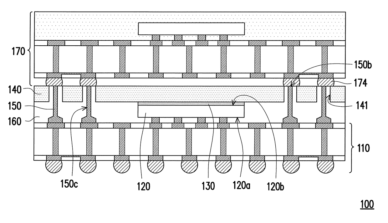
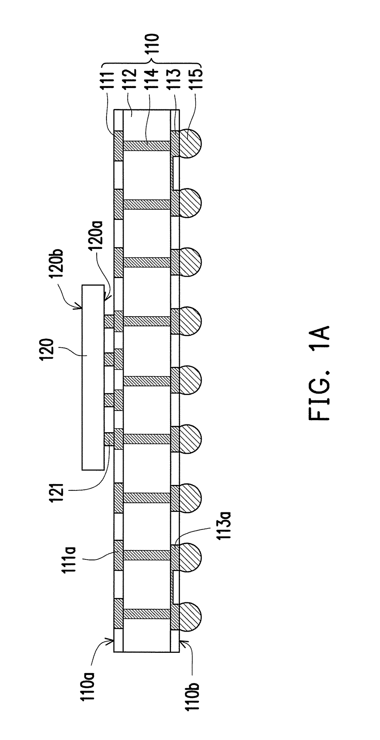
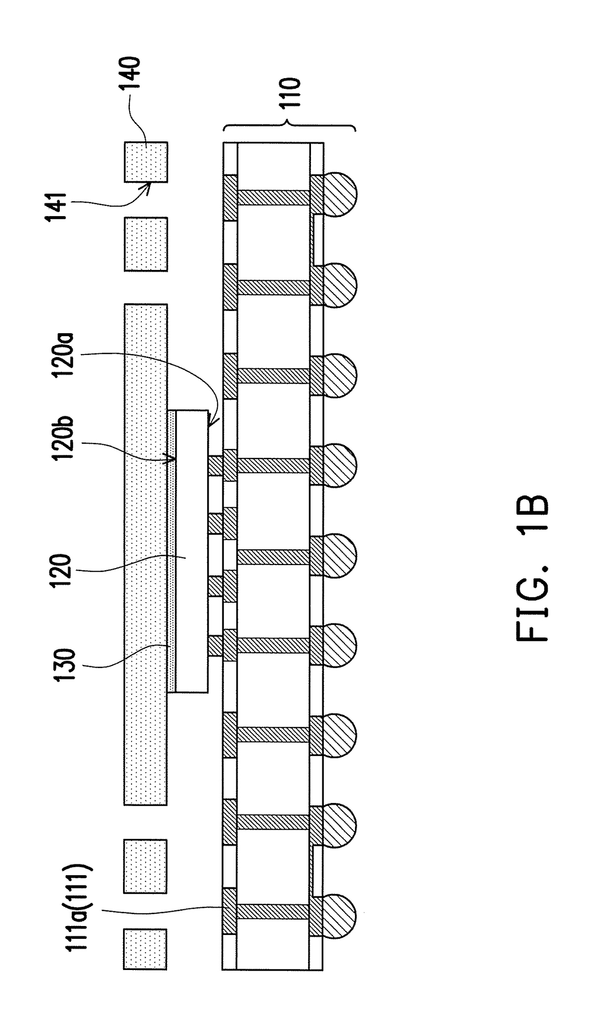
[0015]FIG. 1A to FIG. 1G are cross sections of the manufacturing method of a chip package structure 100 according to an embodiment of the invention. Referring to FIG. 1A, a substrate 110 is provided. The substrate 110 may have a first surface 110a and a second surface 110b opposite to the first surface 110a. The substrate 110 may include a first circuit layer 111, a core layer 112, a second circuit layer 113, and a plurality of vias 114. The first circuit layer 111 is disposed on the first surface 110a, the second circuit layer 113 is disposed on the second surface 110b, and the first circuit layer 111 and the second circuit layer 113 may be electrically connected to each other through the vias 114 p...


PUM


Abstract

A chip package structure including a substrate, a first chip, a frame, a plurality of first conductive connectors, a first encapsulant, and a package is provided. The first chip is disposed on the substrate. The first chip has an active surface and a back surface opposite to the active surface, and the active surface faces the substrate. The frame is disposed on the back surface of the first chip and the frame has a plurality of openings. The first conductive connectors are disposed on the substrate and the first conductive connectors are disposed in correspondence to the openings. The first encapsulant is disposed between the substrate and the frame and encapsulates the first chip. The package is disposed on the frame and is electrically connected to the substrate via the first conductive connectors.

Description

CROSS REFERENCE TO RELATED APPLICATION[0001]This application claims the priority benefit of U.S. provisional application Ser. No. 62 / 410,851, filed on Oct. 21, 2016. The entirety of the above-mentioned patent application is hereby incorporated by reference herein and made a part of specification.BACKGROUND OF THE INVENTIONField of the Invention[0002]The invention relates to a chip package structure and a manufacturing method thereof, and more particularly, to a chip package structure having a frame and a manufacturing method thereof.Description of Related Art[0003]In recent years, electronic equipment and manufacturing techniques meeting increased market demand have been vigorously developed. In consideration of portability and the continuously growing demand of computers, communications products, and consumer electronic products, the traditional single-chip package structure has been failing to meet market demand. In other words, during product design, the characteristics of small ...

Claims


Application Information

Patent Timeline
IPC IPC(8): H01L25/10H01L23/04H01L23/00H01L23/31H01L21/48H01L21/56H01L25/00
CPCH01L25/105H01L23/04H01L24/16H01L23/3128H01L24/32H01L24/83H01L21/4853H01L21/565H01L21/4889H01L24/27H01L24/11H01L25/50H01L24/73H01L24/92H01L2224/16227H01L2224/32225H01L2224/73253H01L2224/92225H01L2225/1023H01L2225/1058H01L23/49827H01L23/49838H01L21/50H01L24/82H01L23/49811H01L23/49816H01L24/48H01L24/81H01L24/85H01L23/3107H01L23/3672H01L25/0657H01L25/18H01L21/561H01L23/3121H01L25/071H01L2224/48091H01L2224/3224H01L2224/85007H01L2224/82047H01L2224/81H01L2224/83007H01L2224/13023H01L2224/16237H01L2225/1088H01L24/13H01L24/29H01L24/45H01L2224/0401H01L2224/04042H01L2224/13147H01L2224/29139H01L2224/2919H01L2224/32245H01L2224/45144H01L2224/45147H01L2224/48227H01L2224/48235H01L2224/73265H01L2225/1094H01L2924/1431H01L2924/1433H01L2924/15311H01L2924/1533H01L23/4334H01L23/42H01L2224/16235H01L2225/1041H01L2924/181H01L2224/08245H01L2224/73251H01L2224/85181H01L2224/85186H01L2224/83101H01L2224/29339H01L2224/29294H01L24/08H01L2224/92222H01L24/80H01L2924/00012H01L2924/00014H01L2224/08H01L2224/16H01L2224/80H01L21/486H01L23/49H01L23/49833H01L23/50H01L2225/1035H01L21/56H01L21/563H01L23/5384H01L24/03H01L24/97H01L2224/03H01L2924/00
Inventor WANG, CHI-ANHSU, HUNG-HSIN
Owner POWERTECH TECHNOLOGY
Why Eureka
Try Eureka