Display device and method for manufacturing the same

Active Publication Date: 2018-05-03
LG DISPLAY CO LTD
View PDF20 Cites 8 Cited by
  • Summary
  • Abstract
  • Description
  • Claims
  • Application Information

AI Technical Summary

Benefits of technology

[0006]The present disclosure provides a display device and a method for manufacturing the same capable of preventing a defective

Problems solved by technology

High heat generated in the large-sized thin film transistor of the GIP driver can be transferred to an organic layer adjacent to the large-sized thin film transistor, thereby causing damage to the organic layer.
Th

Method used


Image

  • Display device and method for manufacturing the same
  • Display device and method for manufacturing the same
  • Display device and method for manufacturing the same

Examples


first example

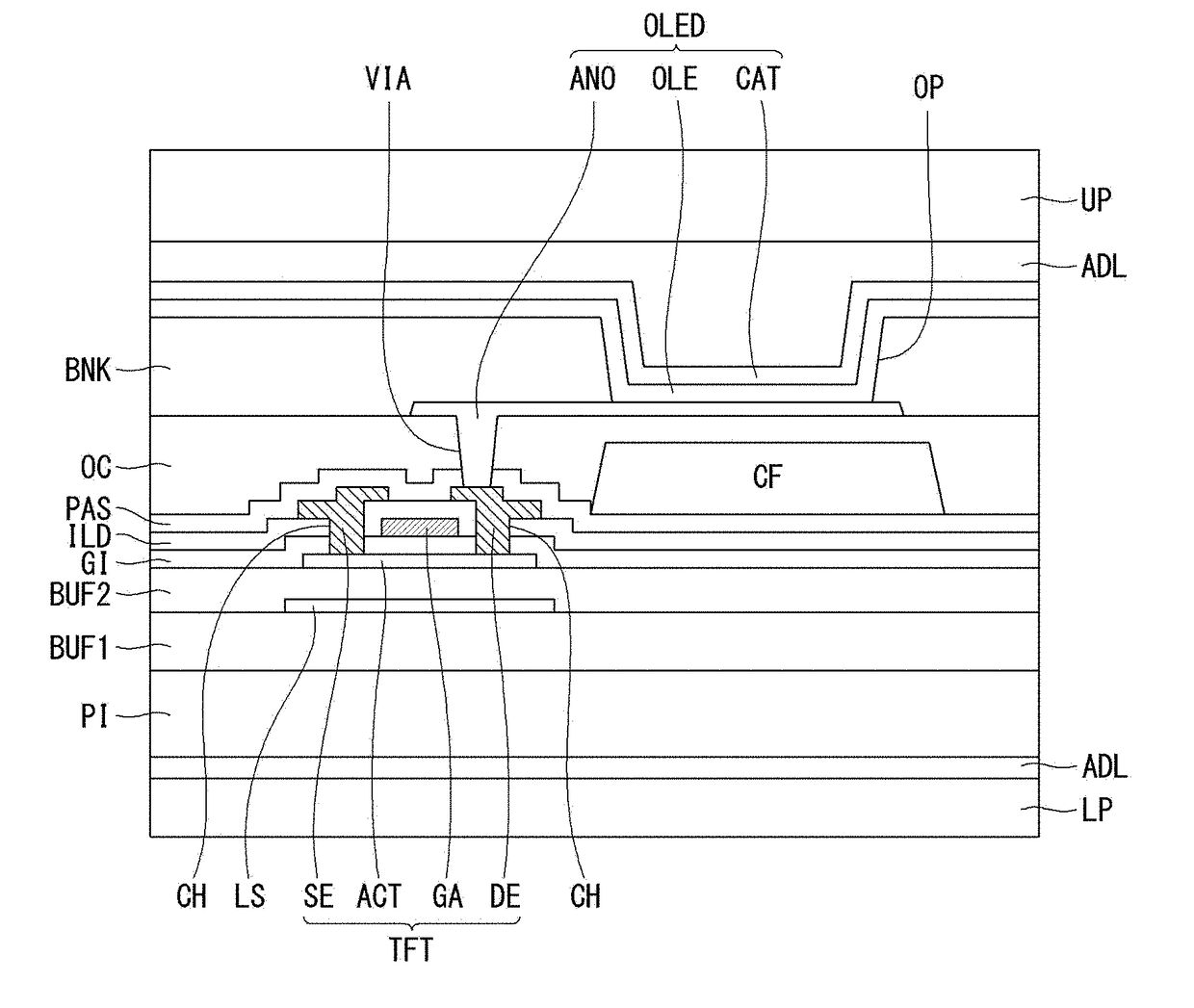
[0050]FIG. 4 is a plan view of an OLED display according to an exemplary aspect. FIG. 5 is a cross-sectional view illustrating a subpixel of an OLED display according to an exemplary aspect. FIG. 6 is a partial enlarged plan view of a portion of FIG. 4. FIG. 7 is a circuit diagram of a gate-in-panel (GIP) driver. FIG. 8 is a cross-sectional view taken along line I-I′ of FIG. 6. FIG. 9 is a plan view illustrating shapes of a heat pad. FIGS. 10 and 11 are cross-sectional views of an OLED display according to another exemplary aspect.

[0051]Referring to FIG. 4, an OLED display includes a flexible substrate PI, a display unit A / A, a GIP driver GIP disposed on a right side of the flexible substrate PI outside the display unit A / A, and a pad portion PD disposed on a lower side of the flexible substrate PI. The display unit A / A may include a plurality of subpixels SP. For example, R (red), G (green), and B (blue) subpixels or R, G, B, and W (white) subpixels of the display unit A / A may emit...


PUM


Abstract

A display device and a method for manufacturing the same capable of preventing a defective drive of a gate-in-panel (GIP) driver by dissipating high heat generated in a large-sized thin film transistor of the GIP driver are disclosed. The display device includes a flexible substrate, a GIP driver and a display unit disposed on the flexible substrate, a protective member disposed under the flexible substrate, and a heat pad disposed between the flexible substrate and the protective member and overlapping the GIP driver.

Description

CROSS REFERENCE TO RELATED APPLICATION[0001]This application claims the priority benefit of Korean Patent Application No. 10-2016-0141015 filed on Oct. 27, 2016, which is incorporated herein by reference in its entirety for all purposes as if fully set forth herein.BACKGROUNDField of the Disclosure[0002]The present disclosure relates to a display device, and more particularly, to a display device and a method for manufacturing the same for preventing damage on thin film transistors.Discussion of the Background[0003]With development of information society, demands for display devices displaying an image are increasing in various ways. In the field of the display devices, a large-sized cathode ray tube (CRT) has been rapidly replaced by a flat panel display (FPD) having advantages of a thin profile, light weight, and a large-sized screen. Examples of the flat panel display include a liquid crystal display (LCD), a plasma display panel (PDP), an organic light emitting diode (OLED) disp...

Claims


Application Information

Patent Timeline
IPC IPC(8): H01L51/52H01L51/00H01L51/56H01L27/32G09G3/3275
CPCH01L51/529H01L51/0097H01L51/003H01L51/56H01L27/3262H01L27/3272H01L27/322G09G3/3275H01L2251/5338H01L2227/326H01L2227/323H01L23/3672H01L27/1218H01L27/1266G09G3/3208G09G2300/0408G09G2330/045G09G2380/02Y02E10/549Y02P70/50H10K59/129H10K59/1213H10K77/111H10K50/87H10K2102/311H10K59/12H10K50/8423H10K50/844H10K59/1201H10K71/00H10K59/38H10K59/126H10K71/80
Inventor KIM, EUNAHYOUN, SANGCHEONLEE, SAEMLEENURI
Owner LG DISPLAY CO LTD
Why Eureka
Try Eureka