
Top-Side Laser for Direct Transfer of Semiconductor Devices

a technology of semiconductor devices and top-side lasers, which is applied in the direction of metal working apparatus, non-electric welding apparatus, manufacturing tools, etc., can solve the problems of 100 times the volume and the inability of circuit assemblies to be thinner

Active Publication Date: 2018-05-24
ROHINNI LLC
View PDF5 Cites 47 Cited by
  • Summary
  • Abstract
  • Description
  • Claims
  • Application Information

AI Technical Summary

Benefits of technology

The patent text describes a process for manufacturing semiconductor devices, which involves preparing semiconductor wafers, dicing them into individual dies, and packaging them for use in various products. The process includes steps such as sorting the dies, connecting them to pins / wires, and sealing them for protection. The resulting circuit assembly cannot be any thinner than the packaging of the semiconductor devices. The patent text also describes a transfer apparatus and a method for transferring semiconductor devices from one location to another. The technical effects of the patent text include improving the efficiency and accuracy of the semiconductor device manufacturing process and facilitating the transfer of semiconductor devices from one location to another.

Problems solved by technology

Additionally, while the packaging of the devices protects them from elements that might degrade or destroy the devices, the packaged devices are inherently larger (e.g., in some cases, around 10 times the thickness and 10 times the area, resulting in 100 times the volume) than the die found inside the package.
Thus, the resulting circuit assembly cannot be any thinner than the packaging of the semiconductor devices.

Method used


Image

  • Top-Side Laser for Direct Transfer of Semiconductor Devices
  • Top-Side Laser for Direct Transfer of Semiconductor Devices
  • Top-Side Laser for Direct Transfer of Semiconductor Devices

Examples


first example embodiment

of a Direct Transfer Apparatus

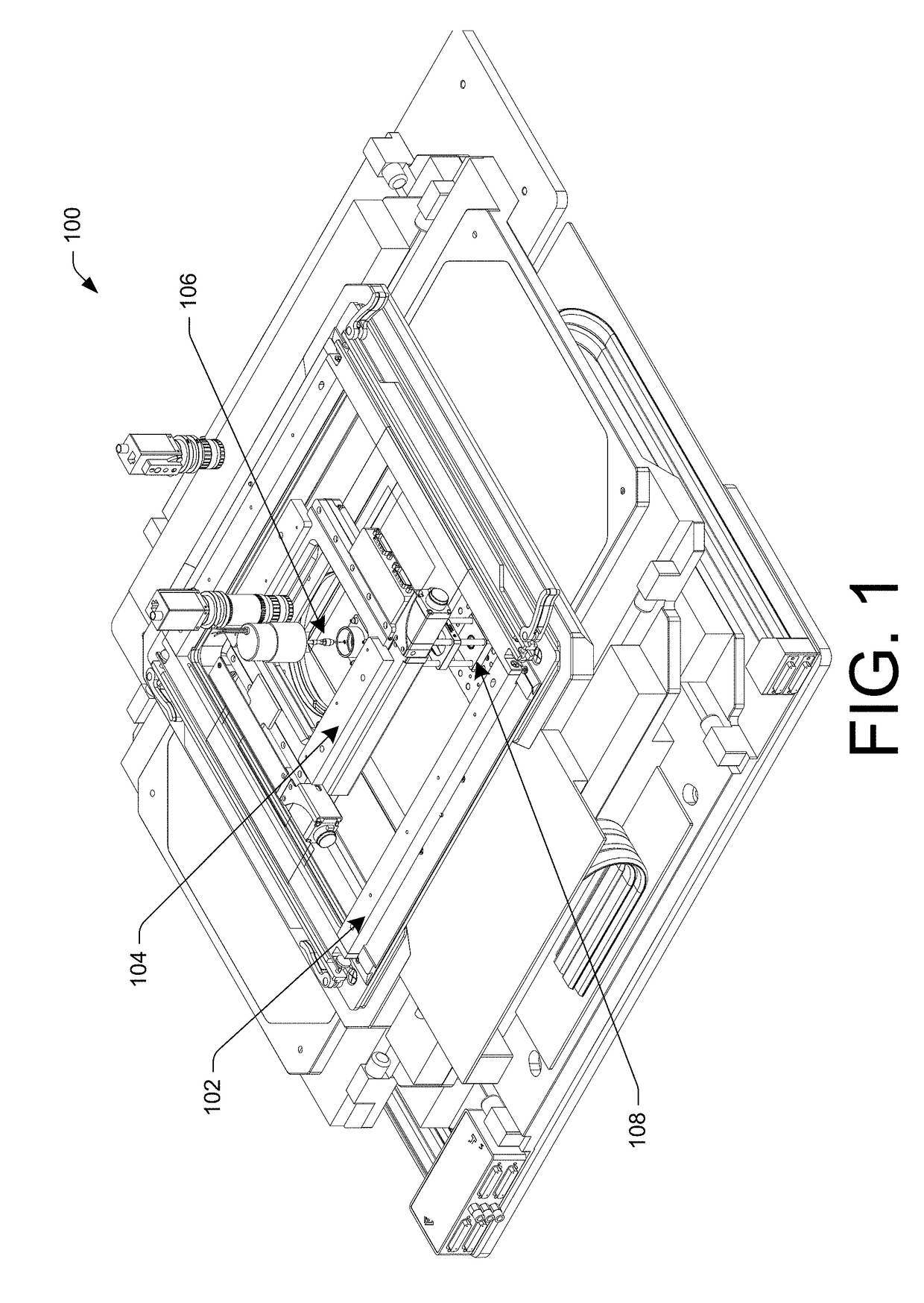
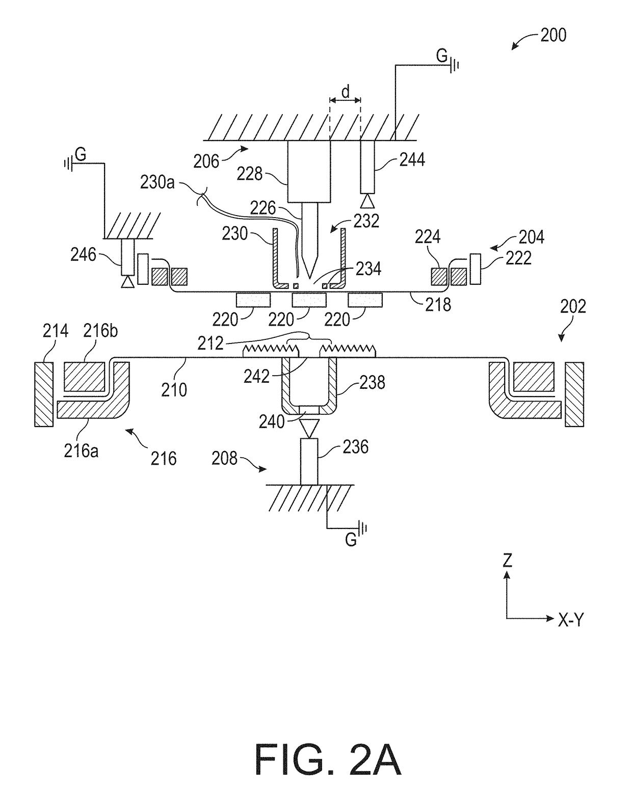
[0040]FIG. 1 illustrates an embodiment of an apparatus 100 that may be used to directly transfer unpackaged semiconductor components (or “dies”) from a wafer tape to a product substrate. The wafer tape may also be referred to herein as the semiconductor device die substrate, or simply a die substrate. The apparatus 100 may include a product substrate conveyance mechanism 102 and a wafer tape conveyance mechanism 104. Each of the product substrate conveyance mechanism 102 and the wafer tape conveyance mechanism 104 may include a frame system or other means to secure the respective substrates to be conveyed to desired alignment positions with respect to each other. The apparatus 100 may further include a transfer mechanism 106, which, as shown, may be disposed vertically above the wafer tape conveyance mechanism 104. In some instances, the transfer mechanism 106 may be located so as to nearly contact the wafer substrate. Additionally, the apparatus 100 ma...

example needle

Actuation Performance Profile

[0083]Illustrated in FIG. 4 is an embodiment of a needle actuation performance profile. That is, FIG. 4 depicts an example of the stroke pattern performed during a transfer operation by displaying the height of the needle tip with respect to the plane of the wafer tape 218 as it varies with time. As such, the “0” position in FIG. 4 may be the upper surface of the wafer tape 218. Further, inasmuch as the idle time of the needle and the ready time of the needle may vary depending on the programmed process or the varying duration of time between transferring a first die and the time it takes to reach a second die for transfer, the dashed lines shown at the idle and ready phases of the stroke pattern indicate that the time is approximate, but may be longer or shorter in duration. Moreover, it is to be understood that the solid lines shown for use of the laser are example times for an embodiment illustrated herewith, however, the actual duration of laser on a...

second example embodiment

of a Direct Transfer Apparatus

[0124]In another embodiment of a direct transfer apparatus, as seen in FIGS. 11A and 11B, a “light string” may be formed. While many of the features of apparatus 1100 may remain substantially similar to those of apparatus 200 of FIGS. 2A and 2B, product substrate conveyance mechanism 1102, as depicted in FIGS. 11A and 11B, may be configured to convey a product substrate 1104 that is different than the product substrate 212. Specifically, in FIGS. 2A and 2B, the product substrate conveyance mechanism 202 includes the conveyor frame 214 and the tensioner frame 216, which secure the sheet-like product substrate 212 under tension. In the embodiment of FIGS. 11A and 11B, however, the product substrate conveyance mechanism 1102 may include a product substrate reel system.

[0125]The product substrate reel system may include one or two circuit trace reels 1106 that are wound with a “string circuit,” which may include a pair of adjacently wound conductive strings...


PUM

PropertyMeasurementUnit
Diameteraaaaaaaaaa
Forceaaaaaaaaaa
Diameteraaaaaaaaaa

Abstract

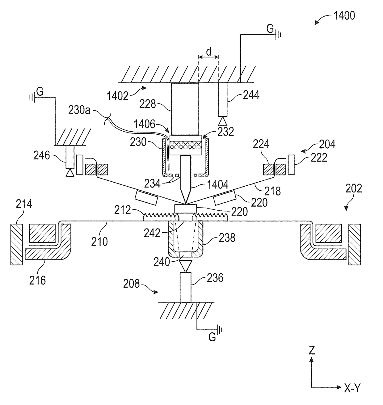
An apparatus includes a needle including a hole extending from a first end to a second end through the needle and an energy-emitting device arranged in the hole of the needle. The energy-emitting device being configured to emit a specific wavelength and intensity of energy directed at an electrically-actuatable element to bond a circuit trace and the electrically-actuatable element.

Description

BACKGROUND[0001]Semiconductor devices are electrical components that utilize semiconductor material, such as silicon, germanium, gallium arsenide, and the like. Semiconductor devices are typically manufactured as single discrete devices or as integrated circuits (ICs). Examples of single discrete devices include electrically-actuatable elements such as light-emitting diodes (LEDs), diodes, transistors, resistors, capacitors, fuses, and the like.[0002]The fabrication of semiconductor devices typically involves an intricate manufacturing process with a myriad of steps. The end-product of the fabrication is a “packaged” semiconductor device. The “packaged” modifier refers to the enclosure and protective features built into the final product as well as the interface that enables the device in the package to be incorporated into an ultimate circuit.[0003]The conventional fabrication process for semiconductor devices starts with handling a semiconductor wafer. The wafer is diced into a mu...

Claims


Application Information

Patent Timeline
IPC IPC(8): B23K26/351H01L21/683H01L21/687B23K26/00B23K26/70B23K26/08
CPCB23K26/351H01L21/6836B23K26/702B23K26/0884B23K26/0054H01L21/6875B23K20/10B23K26/0846B23K26/20B23K2101/42H01L2221/68354H01L24/75H01L21/67132H01L21/67144H01L2924/1203H01L2924/1304H01L2924/12041H01L2224/75262H01L2224/75704H01L2224/75705H01L2224/75303H01L2224/8388H01L2224/83862H01L2224/29339H01L24/29H01L24/83H01L2224/83192H01L2224/83224H01L2224/83205H01L2224/83001H01L2224/759H01L2924/00012H01L2924/00014
Inventor WENDT, JUSTINHUSKA, ANDREWPETERSON, CODY
Owner ROHINNI LLC
Learn More