
Electron-Beam Lithography Method and System

a technology of electron beam and electron beam, which is applied in the direction of microlithography exposure apparatus, electric discharge tubes, instruments, etc., can solve the problems of optical lithography being difficult to improve the size and resolution of the exposure pattern, the lithography has an optical diffraction limit, and the increase of unexpected manufacturing costs, so as to effectively control the proximity effect of an electron beam and effectively control the size and resolution of the development pattern

Active Publication Date: 2018-05-31
NAT TAIWAN UNIV
View PDF0 Cites 0 Cited by
  • Summary
  • Abstract
  • Description
  • Claims
  • Application Information

AI Technical Summary

Benefits of technology

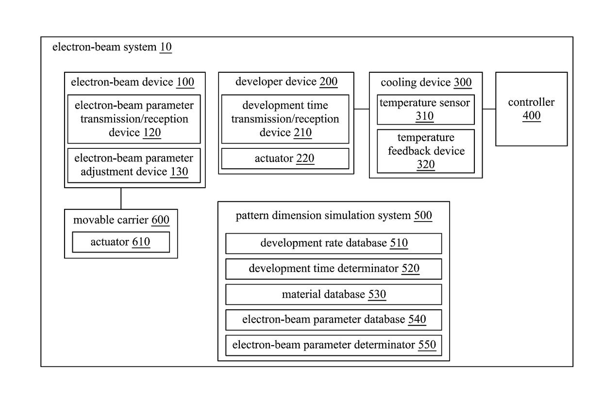
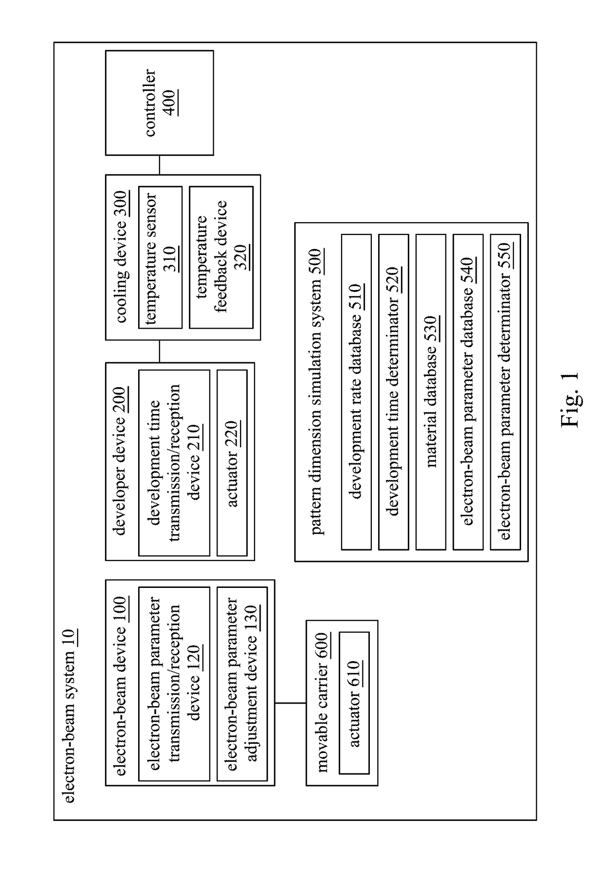
The patent is about a method and system for electron-beam lithography that can control the size and resolution of patterns being developed. It does this by controlling the proximity effect of the electron-beam and by cooling the developer solution to control its dissolution rate. This helps to accurately control the size of the pattern being developed and also reduces the minimum size of the pattern. Overall, the technology allows for more precise and efficient pattern development.

Problems solved by technology

However, the optical lithography has an optical diffraction limit, and thus the optical lithography is difficult to improve a size and a resolution of the exposure pattern.
Furthermore, the optical lithography needs to use different masks for different exposure patterns, thus causing an increase of unexpected manufacture cost.

Method used


Image

  • Electron-Beam Lithography Method and System
  • Electron-Beam Lithography Method and System
  • Electron-Beam Lithography Method and System

Examples


Embodiment Construction

[0017]Reference will now be made in detail to the present embodiments of the disclosure, examples of which are illustrated in the accompanying drawings. Wherever possible, the same reference numbers are used in the drawings and the description to refer to the same or like parts.

[0018]The following disclosure provides many different embodiments, or examples, for implementing different features of the provided subject matter. Specific examples of components and arrangements are described below to simplify the present disclosure. These are, of course, merely examples and are not intended to be limiting. For example, the formation of a first feature over or on a second feature in the description that follows may include embodiments in which the first and second features are formed in direct contact, and may also include embodiments in which additional features may be formed between the first and second features, such that the first and second features may not be in direct contact. In ad...


PUM

PropertyMeasurementUnit
current parameteraaaaaaaaaa
temperatureaaaaaaaaaa

Abstract

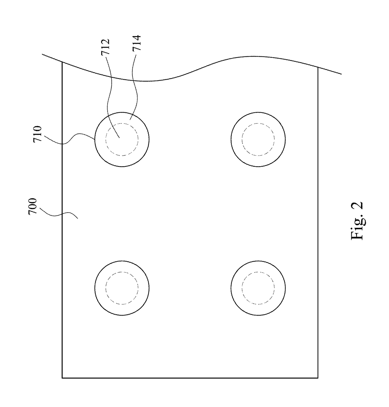
An electron-beam lithography method includes, computing and outputting a development time of a positive-tone electron-sensitive layer and a parameter recipe of an electron-beam device by using a pattern dimension simulation system, performing a low-temperature treatment to chill a developer solution, utilizing an electron-beam to irradiate an exposure region of the positive-tone electron-sensitive layer based on the parameter recipe, and utilizing the chilled developer solution to develop a development region of the positive-tone electron-sensitive layer based on the development time. The development region is present within the exposure region, and an area of the exposure region is smaller than that of the first portion. As a result, the electron-beam lithography method may control a dimension of a development pattern of the positive-tone electron-sensitive layer more accurately, and may also shrink a minimum dimension of the development pattern of the positive-tone electron-sensitive layer.

Description

RELATED APPLICATIONS[0001]This application claims priority to Taiwan Application Serial Number 105139545, filed Nov. 30, 2016, which is herein incorporated by reference.BACKGROUNDTechnical Field[0002]The present disclosure relates to an electron-beam lithography method and an electron-beam lithography system. More particularly, the present disclosure relates to the electron-beam lithography method and system which can control a dimension of a development pattern more accurately.Description of Related Art[0003]In recent years, with the increasing development of semiconductor integrated circuit (IC) industry, technological advances in IC materials and design have produced generations of ICs where each generation has smaller and more complex circuits than its previous generation. In general, the semiconductor IC utilizes an optical lithography to form an exposure pattern. However, the optical lithography has an optical diffraction limit, and thus the optical lithography is difficult to...

Claims


Application Information

Patent Timeline
Patent Type & Authority Applications(United States)
IPC IPC(8): G03F7/20H01J37/317H01J37/30
CPCG03F7/70016H01J37/3174H01J2237/31754H01J2237/2001H01J37/3002H01J2237/31769H01J37/3026
Inventor KUAN, CHIEH-HSIUNGNIEN, CHUNSU, WEN-SHENGCHANG, LI-CHENGCHUNG, CHENG-HUANRAO, WEI-CHENGYEH, HSIU-YUNCHANG, SHAO-WENSHEN, KUAN-YUANONO, SUSUMU
Owner NAT TAIWAN UNIV
Learn More