
Multi-station plasma reactor with RF balancing

a plasma reactor and multi-station technology, applied in the direction of coatings, chemical vapor deposition coatings, electric discharge tubes, etc., can solve the problems of inacceptable variation in the overall process and product, and achieve the effect of reducing the difference between the measurement and the set poin

Active Publication Date: 2018-06-14
LAM RES CORP
View PDF2 Cites 4 Cited by
  • Summary
  • Abstract
  • Description
  • Claims
  • Application Information

AI Technical Summary

Benefits of technology

The patent text discusses a method of controlling the frequency of RF power in a plasma-assisted semiconductor deposition chamber. This can be done by using an RF frequency tuner and RF power adjusters to ensure consistent and reliable results across multiple deposition stations. The method allows for the production of layers with different materials and properties, with precise control over the frequency of the RF power to achieve desired results.

Problems solved by technology

Variation in the processing conditions usually causes variation in deposition and etch rates resulting in unacceptable variation in the overall process and product.

Method used


Image

  • Multi-station plasma reactor with RF balancing
  • Multi-station plasma reactor with RF balancing
  • Multi-station plasma reactor with RF balancing

Examples


Embodiment Construction

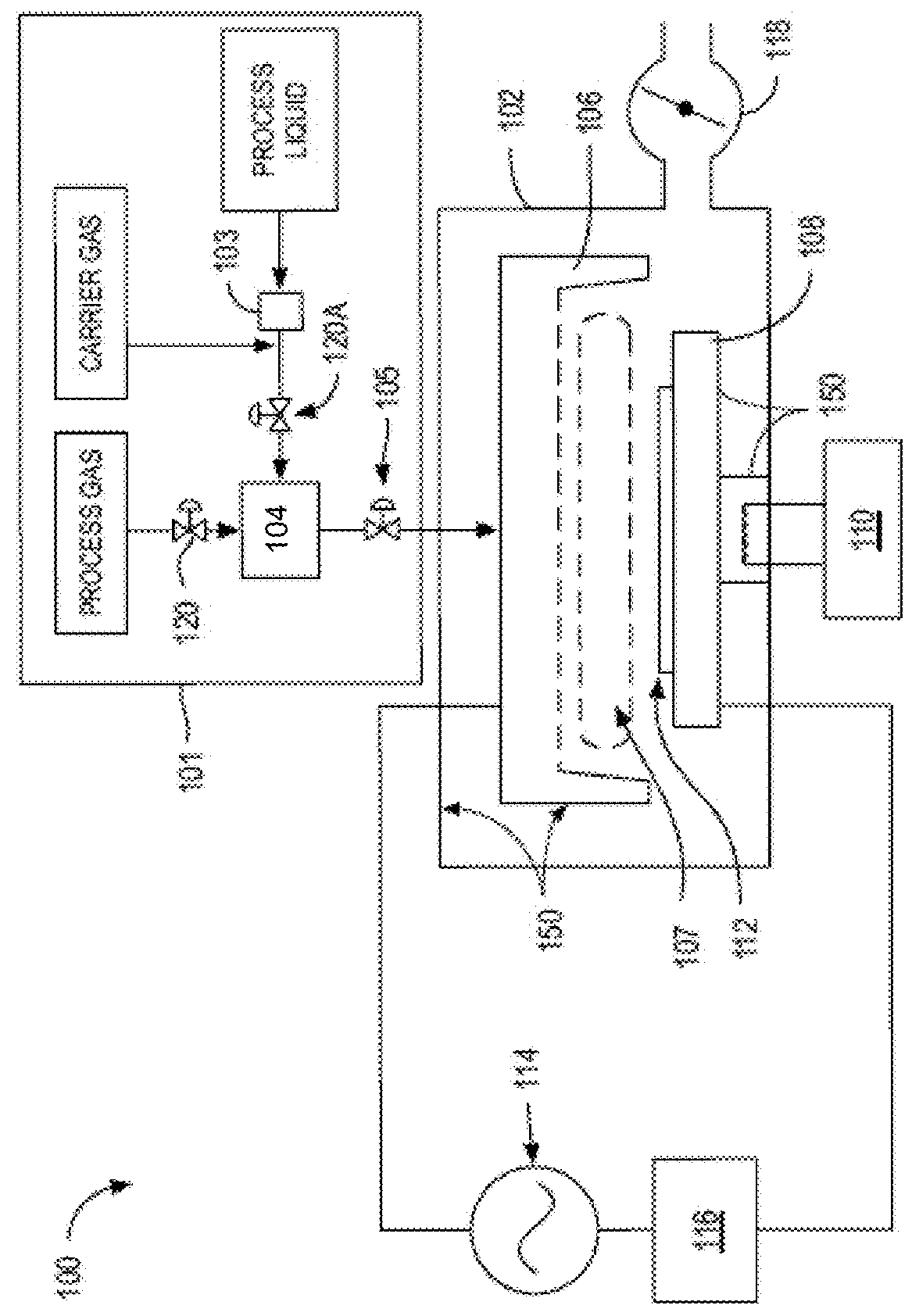
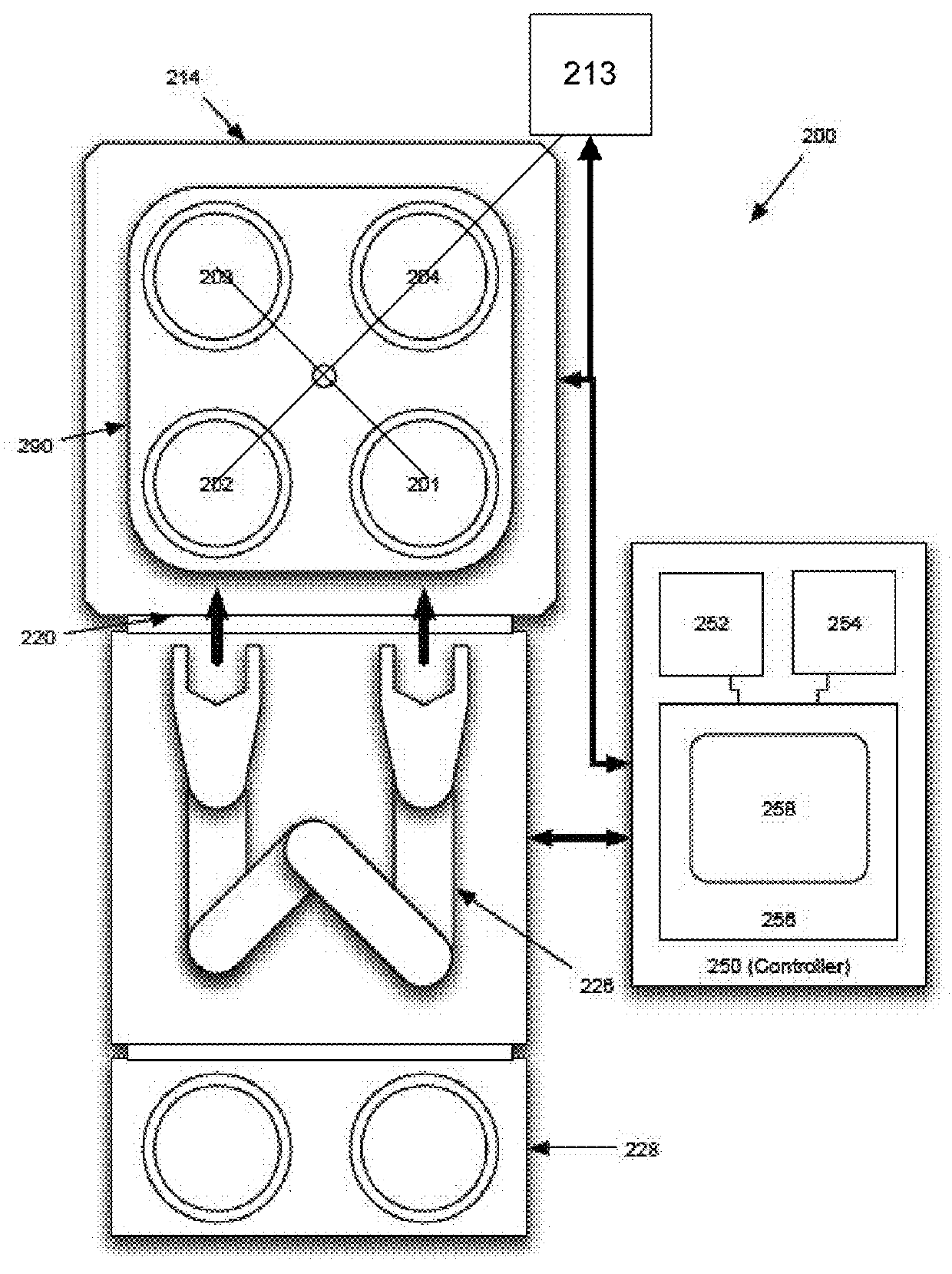
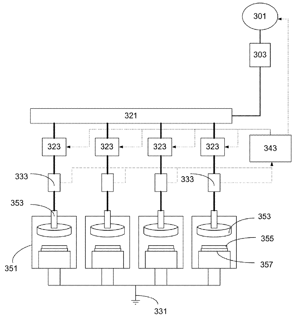
[0025]In the following detailed description, numerous specific implementations are set forth. However, as will be apparent to those skilled in the art, the techniques and apparatus disclosed herein may be practiced without these specific details or by using alternate elements or processes. In other instances, well-known processes, procedures and components have not been described in detail so as not to unnecessarily obscure aspects of the present disclosure.

[0026]Disclosed herein are methods and apparatuses for improving thin film deposition on semiconductor substrates, such as deposition consistency, in semiconductor fabrication operations involving multiple film deposition cycles, each producing a “discrete” film thickness. Atomic layer deposition (ALD) is one such film deposition method, but any technique which puts down thin layers of film and used in a repeating sequential matter may be viewed as involving multiple cycles of deposition, and the methods and apparatuses disclosed...


PUM

PropertyMeasurementUnit
impedanceaaaaaaaaaa
frequencyaaaaaaaaaa
RF frequencyaaaaaaaaaa

Abstract

Apparatuses for multi-station semiconductor deposition operations with RF power frequency tuning are disclosed. The RF power frequency may be tuned according to a measured impedance of a plasma during the semiconductor deposition operation. In certain implementations of the apparatuses, a RF power parameter may be adjusted during or prior to the deposition operation. Certain other implementations of the semiconductor deposition operations may include multiple different deposition processes with corresponding different recipes. The recipes may include different RF power parameters for each respective recipe. The respective recipes may adjust the RF power parameter prior to each deposition process. RF power frequency tuning may be utilized during each deposition process.

Description

CROSS-REFERENCE TO RELATED APPLICATIONS[0001]This application is a divisional of U.S. patent application Ser. No. 14 / 970,337, filed on Dec. 15, 2015 and titled “MULTI-STATION PLASMA REACTOR WITH RF BALANCING,” which itself is a divisional application of U.S. patent application Ser. No. 14 / 458,135, filed on Aug. 12, 2014 and titled “MULTI-STATION PLASMA REACTOR WITH RF BALANCING,” which claims priority benefit under 35 U.S.C. § 119(e) to U.S. Provisional Application No. 62 / 007,350, filed Jun. 3, 2014, titled “MULTI-STATION PLASMA REACTOR WITH RF BALANCING,” all of which are hereby incorporated by reference in their entireties.BACKGROUND[0002]Semiconductor device fabrication involves the processing of semiconductor wafers in a semiconductor processing reactor. Typical processes involve deposition and removal (i.e., etching) of material on the wafer. In commercial scale manufacturing, each wafer contains many copies of a particular semiconductor device being manufactured, and many wafe...

Claims


Application Information

Patent Timeline
Patent Type & Authority Applications(United States)
IPC IPC(8): C23C16/455C23C16/505C23C16/52H01J37/32H01L21/02
CPCC23C16/45544C23C16/45536C23C16/505C23C16/52H01J37/3244H01J37/32082H01J2237/3321H01J37/32183H01J37/32889H01J37/32899H01J37/32935H01J37/32155H01L21/0262C23C16/45538C23C16/45525
Inventor KAPOOR, SUNILLEESER, KARL F.LAVOIE, ADRIENRANGINENI, YASWANTH
Owner LAM RES CORP
Learn More