

Electrooptical device, electronic apparatus, and method for manufacturing electrooptical device
- Summary
- Abstract
- Description
- Claims
- Application Information
AI Technical Summary
Benefits of technology
Problems solved by technology
Method used
Image


Examples
first embodiment
Electrooptical Device
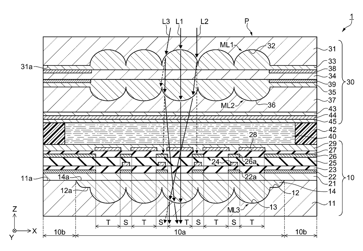
[0059]In a first embodiment, an active matrix type liquid crystal device including a thin film transistor (TFT) as a switching element of a pixel will be described as an example of an electrooptical device. This liquid crystal device, for example, may be suitably used as an optical modulation element (liquid crystal light bulb) of a projection type display apparatus (projector) which will be described later.
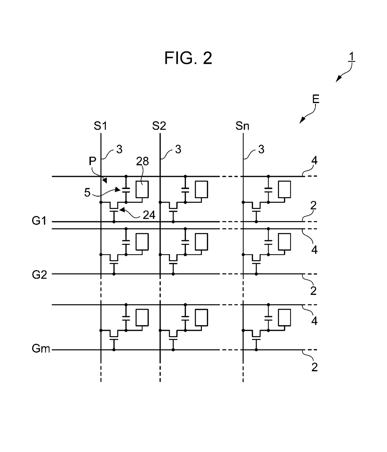
[0060]First, the liquid crystal device as the electrooptical device according to the first embodiment will be described with reference to FIGS. 1 to 3. FIG. 1 is a schematic plan view showing a configuration of the liquid crystal device according to the first embodiment. FIG. 2 is an equivalent circuit diagram showing an electrical configuration of the liquid crystal device according to the first embodiment. FIG. 3 is a schematic sectional view showing a configuration of the liquid crystal device according to the first embodiment. Specifically, FIG. 3 is a sc...
second embodiment
Electronic Apparatus
[0174]Next, the electronic apparatus according to a second embodiment will be described with reference to FIG. 31. FIG. 31 is a schematic view showing a configuration of a projector as the electronic apparatus according to the second embodiment.
[0175]As shown in FIG. 31, a projector (projection type display apparatus) 100 as the electronic apparatus according to the second embodiment includes a polarized light illumination device 110, two dichroic mirrors 104 and 105, three reflecting mirrors 106, 107, and 108, five relay lenses 111, 112, 113, 114, and 115, three liquid crystal light bulbs 121, 122, and 123, a cross dichroic prism 116, and a projection lens 117.
[0176]The polarized light illumination device 110, for example, includes a lamp unit 101 as a light source formed of white light source such as an ultra-high pressure mercury lamp or a halogen lamp, an integrator lens 102, and a polarization conversion element 103. The lamp unit 101, the integrator lens 10...
modification example 1
[0184]In the liquid crystal device 1 according to the first embodiment, the lens surfaces of the microlenses ML1, ML2, and ML3 have a curved surface such as a semicircle or a semiellipse, but the invention is not limited to such a configuration. At least one lens surface of the microlens ML1, ML2, and ML3 may have a flat portion at the center. When the lens surface of microlens includes a flat portion at the center, light incident on the flat portion along the normal direction is transmitted through the microlens without being refracted. Therefore, in a case where parallel light is incident on the liquid crystal device 1, since the parallel light contained in the light emitted from the liquid crystal device 1 increases, the contrast in the projector may be further improved.
PUM
 Abstract
Description
Claims
Application Information