Print circuit board, optical module, and optical transmission equipment
a technology of optical modules and printed circuit boards, applied in the direction of printed circuit non-printed electric components, instruments, waveguides, etc., can solve the problem of unnecessary high frequency noise in such a differential transmission lin
- Summary
- Abstract
- Description
- Claims
- Application Information
AI Technical Summary
Benefits of technology
Problems solved by technology
Method used
Image
Examples
first embodiment
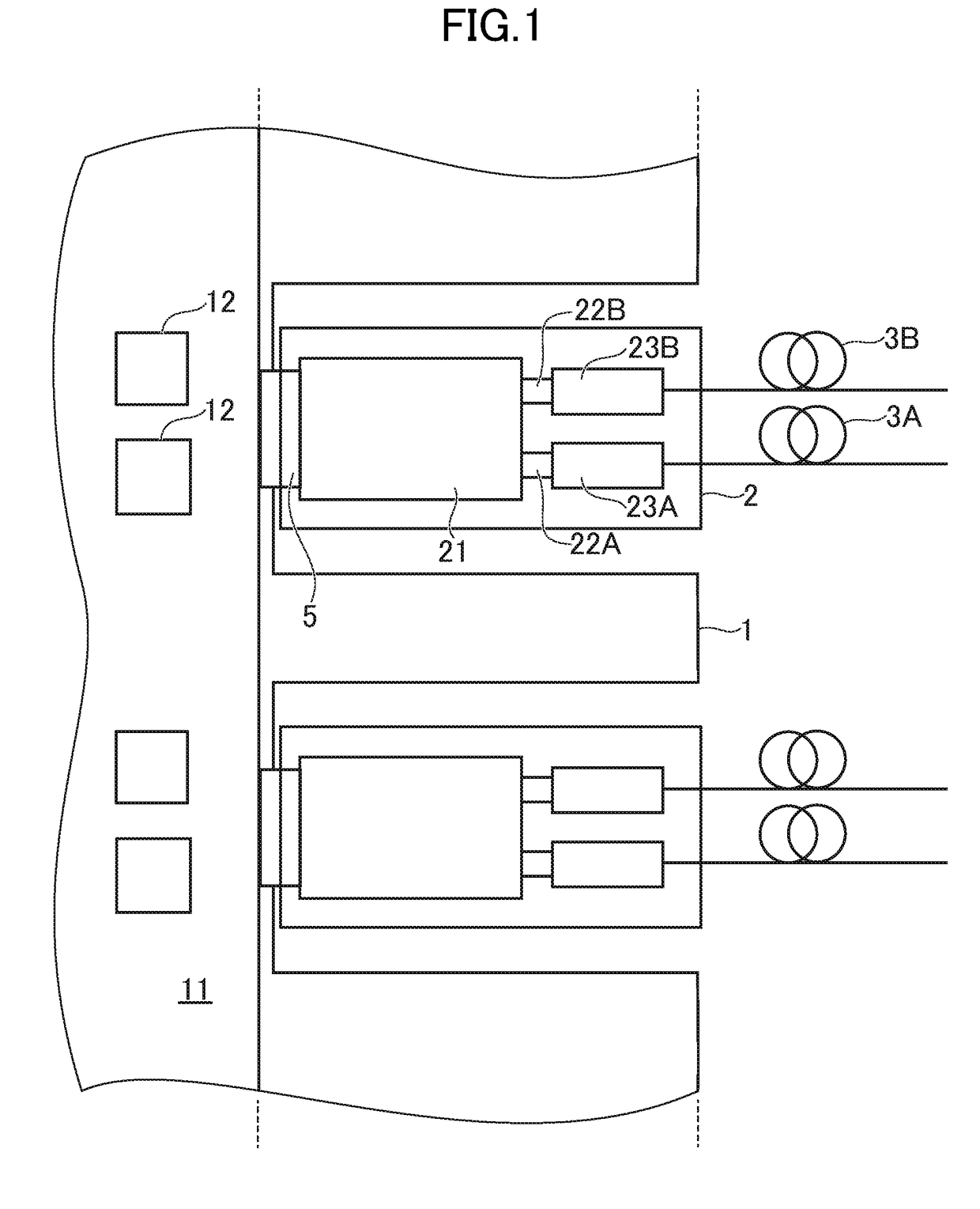
[0042]FIG. 1 is a schematic view illustrating a configuration of an optical transmission equipment 1 and an optical module 2 according to a first embodiment of the present invention. The optical transmission equipment 1 includes a print circuit board 11. In addition, the optical module 2 includes a print circuit board 21. The print circuit board according to the first embodiment is one or both of the print circuit boards 11 and 21.
[0043]The optical transmission equipment 1 further includes an IC 12. The optical transmission equipment 1 is, for example, a large-capacity router or a switch. The optical transmission equipment 1 has, for example, a function of a switching equipment, and is disposed in a base station or the like. The optical transmission equipment 1 acquires data for receiving (electric signal for receiving) from the optical module 2, determines to transmit what data to where using the IC 12 or the like, generates data for transmitting (electric signal for transmitting),...
second embodiment
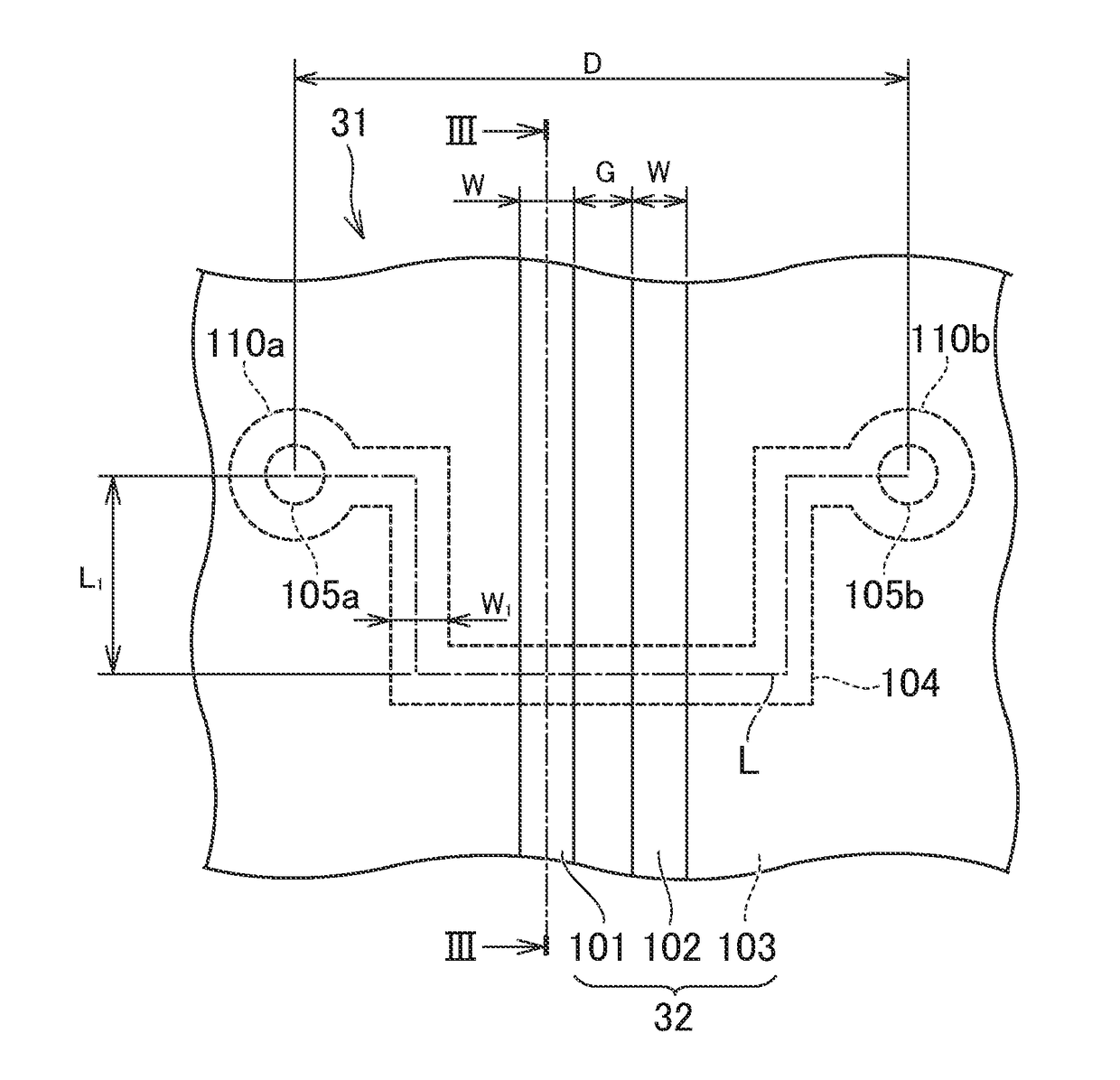
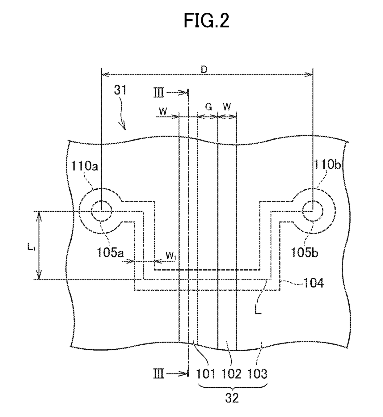
[0083]FIG. 7 is a schematic view illustrating a flat surface of a portion of a print circuit board 31 according to a second embodiment of the present invention. FIG. 8 is a diagram illustrating characteristics of a differential transmission line 32 according to the second embodiment. FIG. 8 illustrates the common mode pass characteristic (Scc 21) of the differential transmission line 32 according to the second embodiment, and the common mode pass characteristic (Scc 21) of the differential transmission line 32 according to the first embodiment of the present invention for comparison. Although the print circuit board 31 according to the second embodiment is different from the first embodiment in that the print circuit board 31 further includes a second resonator conductor 114 and second via holes 115a and 115b in addition to the first resonator conductor 104, the other structure is the same as that of the first embodiment.
[0084]The second resonator conductor 114 is disposed in the sa...
third embodiment
[0088]FIG. 11 is a schematic view illustrating a flat surface of a portion of a print circuit board 31 according to a third embodiment of the present invention. FIG. 12 is a diagram illustrating characteristics of a differential transmission line 32 according to the third embodiment. FIG. 12 illustrates the common mode pass characteristic (Scc 21) of the differential transmission line 32 according to the third embodiment, and the common mode pass characteristic (Scc 21) of the differential transmission line 32 according to the first embodiment of the present invention for comparison. Although in the print circuit board 31 according to the third embodiment, the shape of the second resonator conductor 114 is different from that of the second embodiment, the other structure is the same as that of the second embodiment.
[0089]In the second embodiment, the planar shape of the second resonator conductor 114 is substantially line symmetric with the plane shape of the first resonator conduct...
PUM
 Abstract
Description
Claims
Application Information


