Probe for localized neural optogenetics stimulation and neurochemistry recordings

a localized neural and optogenetics technology, applied in the field of optogenetics, can solve problems such as damage to neurons

Active Publication Date: 2018-07-12
IBM CORP
View PDF10 Cites 10 Cited by
  • Summary
  • Abstract
  • Description
  • Claims
  • Application Information

AI Technical Summary

Problems solved by technology

A challenge with this technology is achieving a highly localized stimulated area (i.e., a small population of neurons).
However, such electrical stimulation is not necessarily specific to a neural circuit and can damage neurons as far as 500 microns away from the stimulation site.

Method used


Image

  • Probe for localized neural optogenetics stimulation and neurochemistry recordings
  • Probe for localized neural optogenetics stimulation and neurochemistry recordings
  • Probe for localized neural optogenetics stimulation and neurochemistry recordings

Examples


first embodiment

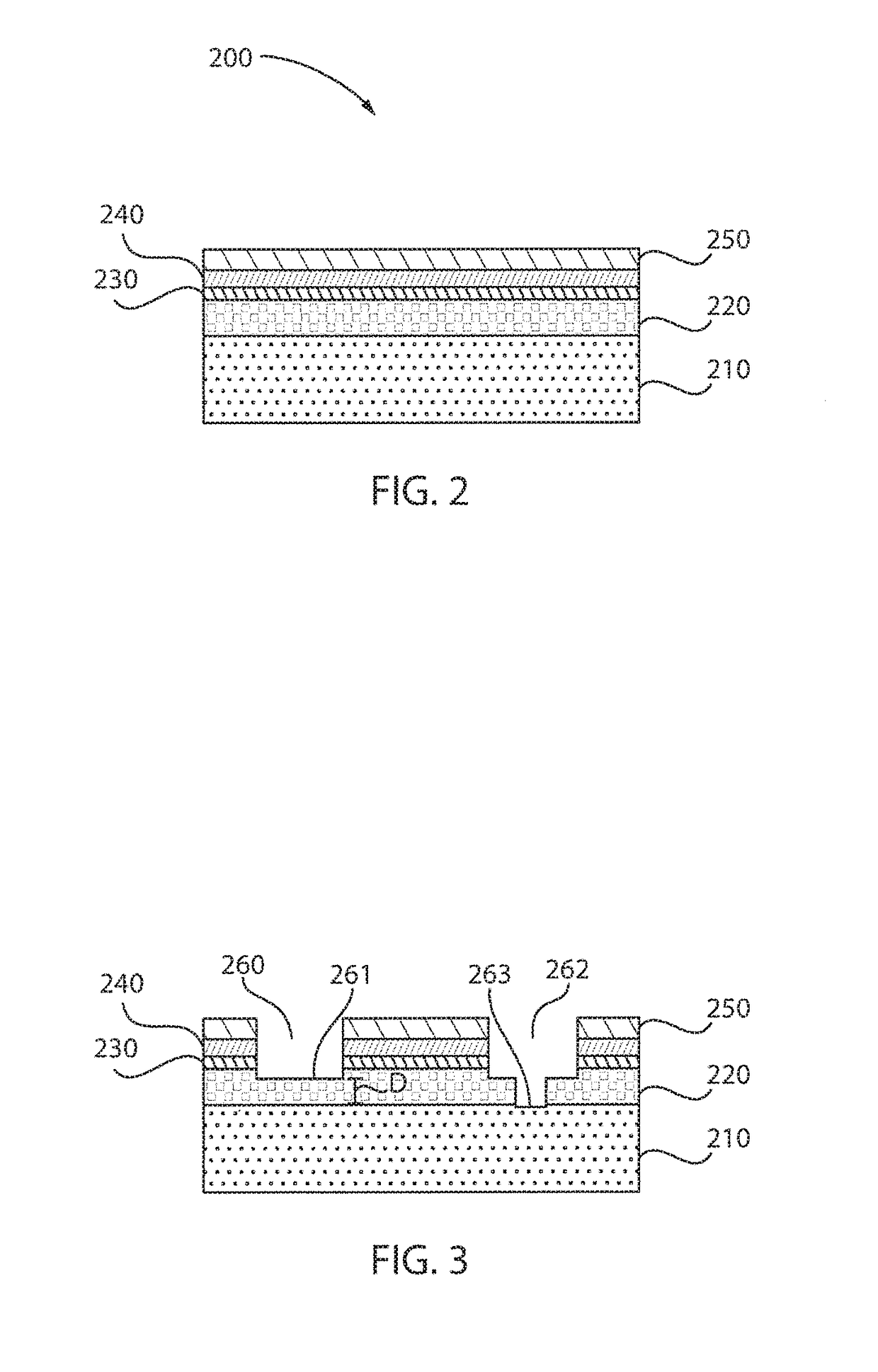
[0102]In a first embodiment, a carbon electrode sensor structure 400 includes a titanium (Ti) or nickel (Ni) layer 410 that is formed over the substrate 405. The substrate 405 can be, e.g., a Si substrate. Segmentation channels 425 are formed such that portions of the substrate 405 are exposed. A vertically aligned CNT or CNF layer 420 is grown over portions of the layers 410 (Ti or Ni). If Ti is used, the Ti layer 410 can have a thickness of about 200 nm. If Ni is used, the Ni layer 410 can have a thickness of about 20 nm. One skilled in the art can contemplate using other types of materials, such as, but not limited to TiN or Ni45Fe55. If TiN is used, the TiN layer 410 can have a thickness of about 200 nm. If Ni45Fe55 is used, the Ni45Fe55 layer 410 can have a thickness of about 20 nm.

second embodiment

[0103]In a second embodiment, a carbon electrode sensor structure 400 includes a titanium (Ti) or gold (Au) layer 410 that is formed over the substrate 405. In this example embodiment, a vertically aligned CNF layer 420 is grown. After deposition of the layer 420, a negative photoresist (not shown) is applied thereto via, e.g., spinning. The negative photoresist can be, e.g., SU-8. Negative refers to a photoresist whereby the parts exposed to UV become cross-linked, while the remainder of the film remains soluble and can be washed away during development. Subsequently, segmentation channels are formed and polystyrene beads are applied on the photoresist. The beads can be, e.g., 1 μm in thickness. Next, a plasma etch can take place, as well as ultrasonification to remove the beads. The CNF layer 420 is then pyrolyzed. Pyrolization can be performed at, e.g., 900° C.

[0104]If Ti is used, the Ti layer 410 can have a thickness of about 200 nm. If Au is used, the Au layer 410 can have a th...


PUM


Abstract

A neural probe is presented for local neural optogenetics stimulation and neurochemistry recordings. The neural probe includes a probe body, a shank extending from the probe body to a tip, a plurality of micro light-emitting diodes (LEDs) positioned across a length of a first surface of the shank for providing neuron-affecting light, a plurality of carbon devices, and a plurality of carbon electrodes positioned across a length of a second surface of the shank, the second surface in opposed relation to the first surface. The plurality of carbon electrodes can be vertically aligned carbon nanotubes or vertically aligned carbon nanofibers. The plurality of carbon electrodes can also be horizontally aligned carbon nanotubes. The plurality of micro LEDs activate neurons and the plurality of vertically aligned carbon electrodes electrochemically record neurotransmitters.

Description

BACKGROUNDTechnical Field[0001]The present invention relates generally to optogenetics, and more specifically, to a neural probe for performing localized neural optogenetics stimulation and neurochemistry recordings at the same time.Description of the Related Art[0002]Electrical neural stimulation and modulation is important in many basic science applications, as well as many clinical applications. Some of the approved electrical stimulators include artificial cardiac pacemakers, cochlear implants, and deep brain stimulation electrodes. A challenge with this technology is achieving a highly localized stimulated area (i.e., a small population of neurons).[0003]Massively-parallel access to the activity of large populations of individual neurons with high spatial and temporal resolution has been a long-sought goal in neuroscience. With advances in microelectromechanical systems (MEMS) and microelectronics, there has been progress toward this goal as planar fabrication processes have be...

Claims


Application Information

Patent Timeline
Patent Type & Authority Applications(United States)
IPC IPC(8): A61N5/06A61B5/04
CPCA61N5/0622A61N2005/0651A61N5/0601A61B5/04001A61B2562/0209A61N2005/0612A61N2005/0652A61N2005/0653A61N2005/0659A61N2005/0663A61B5/24
Inventor DELIGIANNI, HARIKLIAHAN, SHU-JENSPROGIS, EDMUND J.
Owner IBM CORP
Why Eureka
Try Eureka