Resistive Change Elements Incorporating Carbon Based Diode Select Devices
What is Al technical title?
Al technical title is built by PatSnap Al team. It summarizes the technical point description of the patent document.
a technology of resistive change elements and select devices, which is applied in the direction of digital storage, semiconductor devices, instruments, etc., can solve the problems of low fabrication cost and very little power consumption
Active Publication Date: 2018-07-12
NANTERO
View PDF0 Cites 14 Cited by
Summary
Abstract
Description
Claims
Application Information
AI Technical Summary
This helps you quickly interpret patents by identifying the three key elements:
Problems solved by technology
Method used
Benefits of technology
Problems solved by technology
A resistive change memory device has resistive change memory elements that are scalable to very high densities, incur very low fabrication costs, store nonvolatile memory states, and consume very little power.
Method used
Image
Click on the blue label to locate the original text in one second.
Reading with bidirectional positioning of images and text.
Examples
Embodiment Construction
NRAM and Cross Point Memory Cells
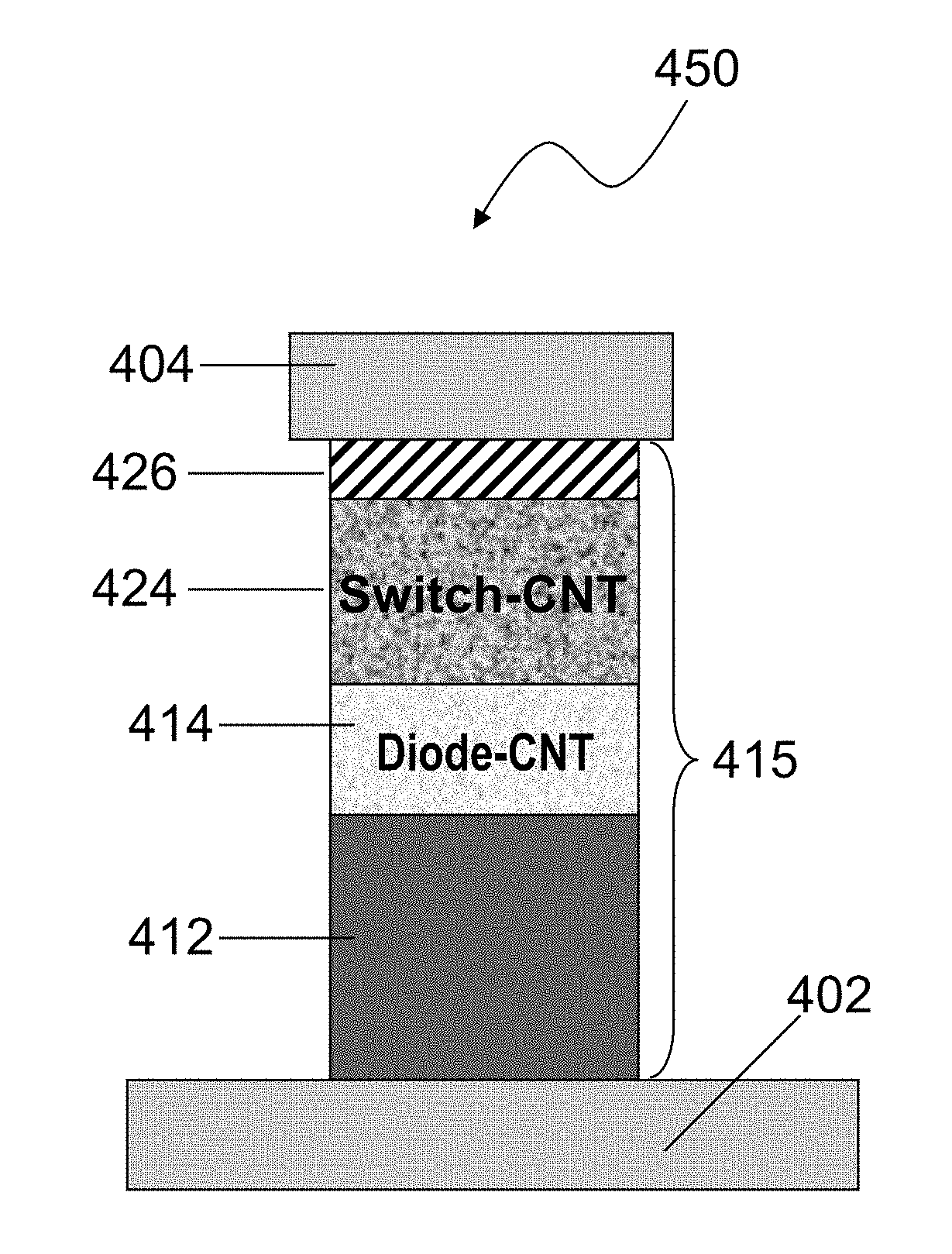
[0169]The present disclosure is generally directed toward nonvolatile resistive change memory cells (or elements) forming 1-R memory cells in a cross point cell configuration, approximately 4 F2 in area, with cell select and nonvolatile storage functions combined in a single element. Nonvolatile resistive change memory elements using carbon layers as storage elements can form cross point nonvolatile resistive memory elements. In the present disclosure, the term carbon layer is defined as any allotrope of carbon, excluding amorphous carbon.
[0170]To elaborate further, a carbon layer as referred to herein for the present disclosure includes a layer of multiple, interconnected carbon structures (such as, but not limited to, carbon nanotubes, graphite, buckyballs, and nanocapsules) formed in a layer such as to provide at least one electrically conductive path through the layer. The carbon layer can be, for example, a nanotube fabric (as described in detai...
PUM
Abstract
The present disclosure is directed toward carbon based diodes, carbon based resistive change memory elements, resistive change memory having resistive change memory elements and carbon based diodes, methods of making carbon based diodes, methods of making resistive change memory elements having carbon based diodes, and methods of making resistive change memory having resistive change memory elements having carbons based diodes. The carbon based diodes can be any suitable type of diode that can be formed using carbon allotropes, such as semiconducting single wall carbon nanotubes (s-SWCNT), semiconducting Buckminsterfullerenes (such as C60 Buckyballs), or semiconducting graphitic layers (layered graphene). The carbon based diodes can be pn junction diodes, Schottky diodes, other any other type of diode formed using a carbon allotrope. The carbon based diodes can be placed at any level of integration in a three dimensional (3D) electronic device such as integrated with components or wiring layers.
Description
[0001]This application is a continuation of U.S. Pat. No. 9,917,139, entitled “Resistive Change Element Array using Vertically Oriented Bit Lines,” filed Dec. 20, 2016, which is a continuation of U.S. Pat. No. 9,783,255, entitled “Cross Point Arrays of 1-R Nonvolatile Resistive Change Memory Cells Using Continuous Nanotube Fabrics,” filed Jun. 29, 2016, which is a continuation of U.S. Pat. No. 9,390,790, entitled “Carbon Based Nonvolatile Cross Point Memory Incorporating Carbon Based Diode Select Devices and MOSFET Select Devices for Memory and Logic Applications,” filed Dec. 17, 2012.CROSS-REFERENCE TO RELATED APPLICATIONS[0002]This application is related to the following U.S. patents, which are assigned to the assignee of the present application, and are hereby incorporated by reference in their entirety:[0003]U.S. Pat. No. 6,574,130, filed Jul. 25, 2001, entitled “Hybrid Circuit Having Nanotube Electromechanical Memory;”[0004]U.S. Pat. No. 6,643,165, filed Jul. 25, 2001, entitled...
Claims
Application Information
Patent Timeline
Application Date:The date an application was filed.
Publication Date:The date a patent or application was officially published.
First Publication Date:The earliest publication date of a patent with the same application number.
Issue Date:Publication date of the patent grant document.
PCT Entry Date:The Entry date of PCT National Phase.
Estimated Expiry Date:The statutory expiry date of a patent right according to the Patent Law, and it is the longest term of protection that the patent right can achieve without the termination of the patent right due to other reasons(Term extension factor has been taken into account ).
Invalid Date:Actual expiry date is based on effective date or publication date of legal transaction data of invalid patent.
Patent Type & Authority Applications(United States)