
Component Having a Metal Carrier and Method for Producing Components

a metal carrier and component technology, applied in the direction of basic electric elements, electrical apparatus, semiconductor devices, etc., can solve the problems of insufficient mechanical stability of the molded potential risk of the molded body made of plastic, and insufficient mechanical stability of the molded body, so as to achieve high mechanical and thermal stability and cost-effective

Active Publication Date: 2018-08-02
OSRAM OLED
View PDF7 Cites 0 Cited by
  • Summary
  • Abstract
  • Description
  • Claims
  • Application Information

AI Technical Summary

Benefits of technology

The patent provides a component that is stable and can withstand high bending loads. The method of producing the component is cost-effective because it involves using a single-piece structure with a high thickness of the carrier layer. This structure provides a broad mechanical support and allows the component to withstand high bending loads. The insulating layer and through-contact can be formed on the carrier layer which is formed directly on the semiconductor body, reducing production costs. The carrier is formed in the presence of the semiconductor body, which can be carried out at wafer level before singulation, resulting in lower costs for the components.

Problems solved by technology

An optoelectronic component comprising a carrier, which contains a molded body made of a plastic, has an insufficient mechanical stability at least in places.
With regard to thermal resilience and cycle stability, in particular with regard to cyclic temperature changes, the molded body made of a plastic, for instance, made from a casting compound, poses a potential risk.

Method used


Image

  • Component Having a Metal Carrier and Method for Producing Components
  • Component Having a Metal Carrier and Method for Producing Components
  • Component Having a Metal Carrier and Method for Producing Components

Examples


Embodiment Construction

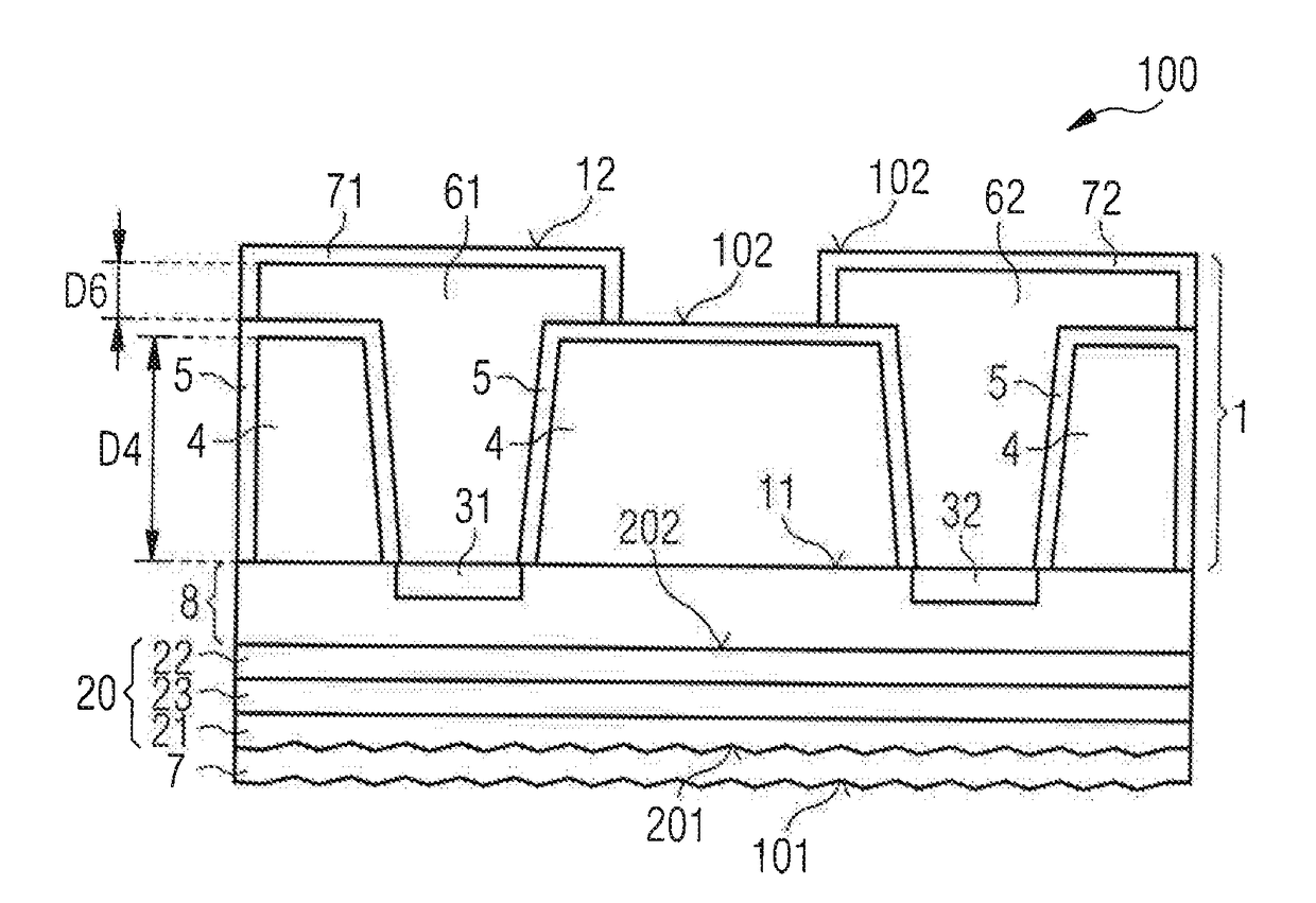
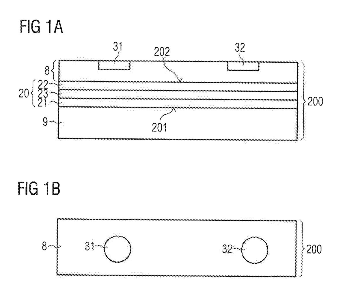
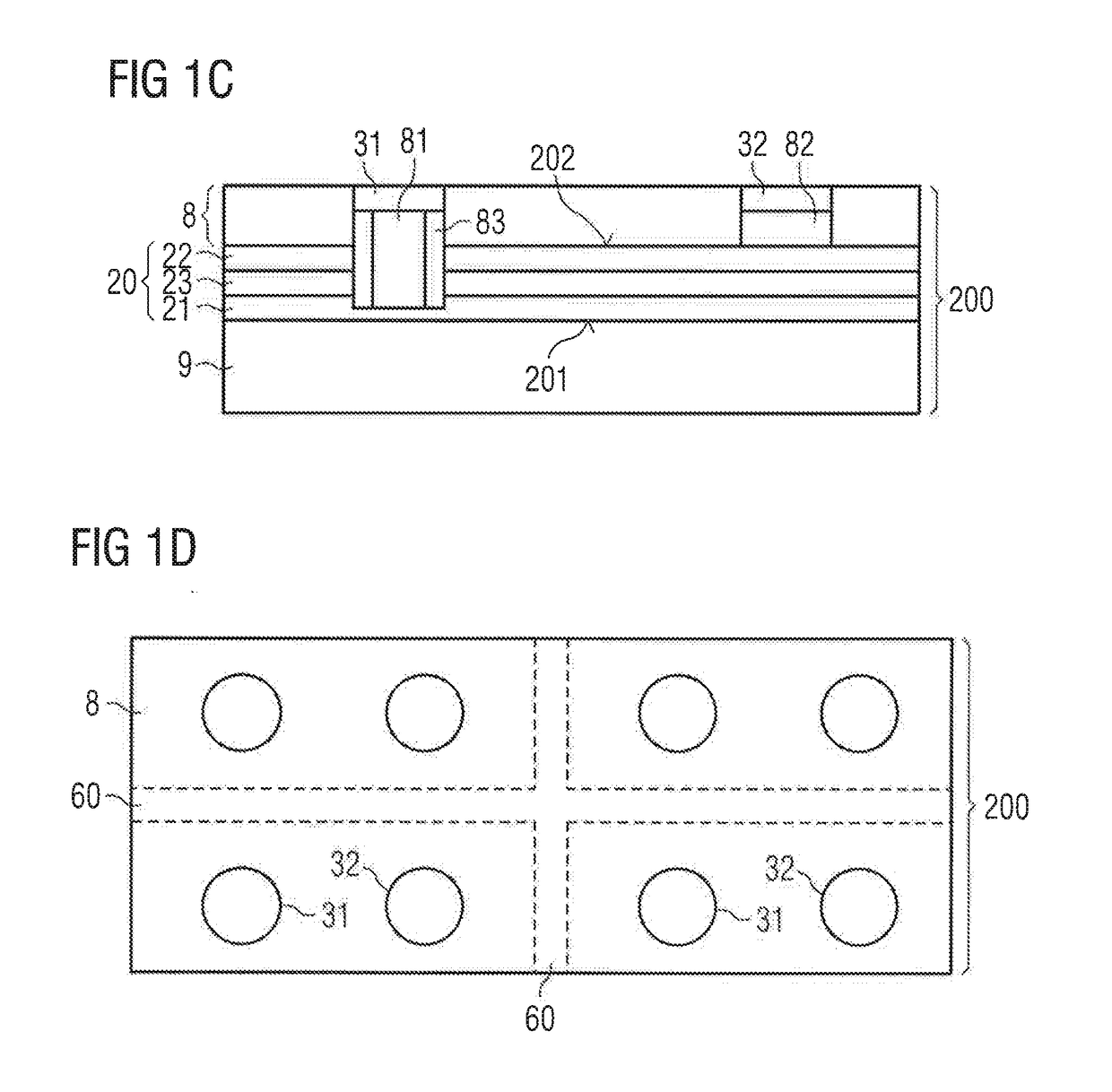
[0037]A composite 200 is shown in FIG. 1A. In particular, the composite 200 is a wafer composite. The composite 200 has a semiconductor composite 20. The semiconductor composite 20 is arranged on a substrate 9. In particular, the substrate 9 is a growth substrate, for example, a sapphire substrate, wherein the semiconductor composite 20 is preferably grown layerwise on the substrate 9 by means of an epitaxy method. The growth direction is in particular perpendicular to a main plane of extension of the substrate 9. In particular, the growth direction is perpendicular to a first main surface 201 and / or a second main surface 202 of the semiconductor composite 20. In FIG. 1A, the first main surface 201 faces towards the substrate 9 and the second main surface 202 faces away from the substrate 9.

[0038]The semiconductor composite 20 can be formed from a III / V compound semiconductor material. An III / V compound semiconductor material has an element from the third main group, such as B, Al, ...


PUM


Abstract

A component having a metal carrier and a method for producing a component are disclosed. In an embodiment the component includes a carrier having a metallic carrier layer, an insulating layer and a first through-contact extending in a vertical direction throughout the carrier layer, wherein the through-contact is electrically isolated from the carrier layer via the insulating layer. The component further includes a semiconductor body and a wiring structure arranged in the vertical direction between the carrier and the semiconductor body at least places and electrically contacting the semiconductor body, wherein the wiring structure has a first connection area and a second connection area, wherein the connection areas adjoin the carrier and are assigned to different electrical polarities of the component, wherein the first through-contact is in electrical contact with one of the connection areas, and wherein the component is configured to be externally electrically connectable via the carrier.

Description

[0001]This patent application is a national phase filing under section 371 of PCT / EP2016 / 066810, filed Jul. 14, 2016, which claims the priority of German patent application 10 2015 112 280.4, filed Jul. 28, 2015, each of which is incorporated herein by reference in its entirety.TECHNICAL FIELD[0002]A component having a metal carrier and a method for producing a plurality of components are provided.BACKGROUND[0003]An optoelectronic component comprising a carrier, which contains a molded body made of a plastic, has an insufficient mechanical stability at least in places. With regard to thermal resilience and cycle stability, in particular with regard to cyclic temperature changes, the molded body made of a plastic, for instance, made from a casting compound, poses a potential risk.SUMMARY OF THE INVENTION[0004]Embodiments provide a component having a high mechanical and thermal stability. Further embodiments provide a cost-effective method for producing one or a plurality of component...

Claims


Application Information

Patent Timeline
IPC IPC(8): H01L33/48H01L33/62H01L33/44H01L33/30
CPCH01L33/486H01L33/62H01L33/44H01L33/30H01L2933/0025H01L2933/0066H01L2224/11
Inventor LEIRER, CHRISTIANSCHWARZ, THOMASHOPPEL, LUTZ
Owner OSRAM OLED
Learn More