Layout of optical engine components and integrated circuits on a transceiver printed circuit board

Active Publication Date: 2018-09-06
FOXCONN INTERCONNECT TECHNOLOGY LIMITED
View PDF9 Cites 0 Cited by
  • Summary
  • Abstract
  • Description
  • Claims
  • Application Information

AI Technical Summary

Benefits of technology

[0005]An object of the present invention is to provide a transceiver having an improving printed circui

Problems solved by technology

Traditionally, typically one of the most expensive components in a fiber optics transceiver is the total silicon content used for the LD IC, TIA IC, and CDR IC.
However doing so does have its challenges.
A fully combined single-IC solution would then need

Method used


Image

  • Layout of optical engine components and integrated circuits on a transceiver printed circuit board
  • Layout of optical engine components and integrated circuits on a transceiver printed circuit board
  • Layout of optical engine components and integrated circuits on a transceiver printed circuit board

Examples


first embodiment

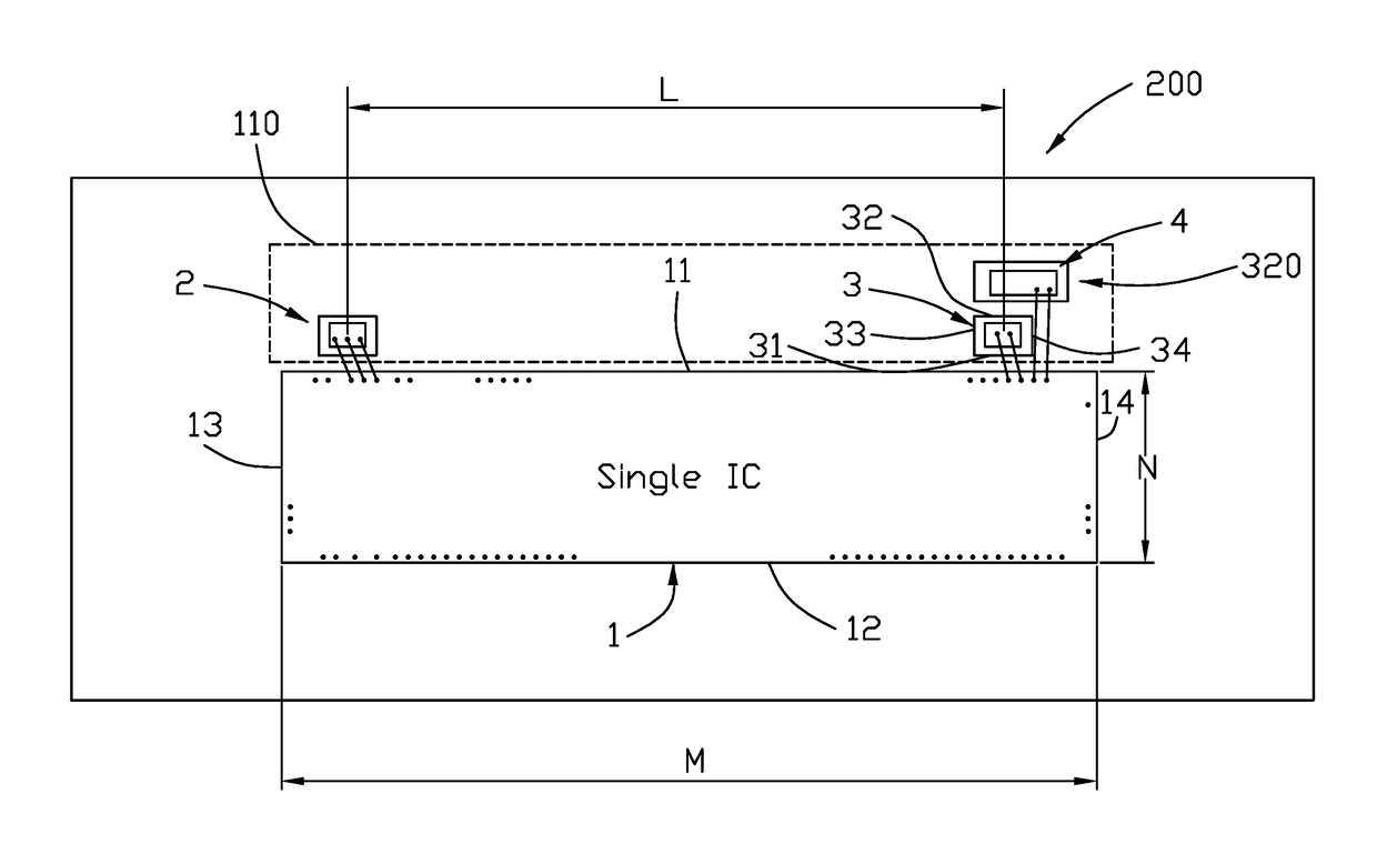
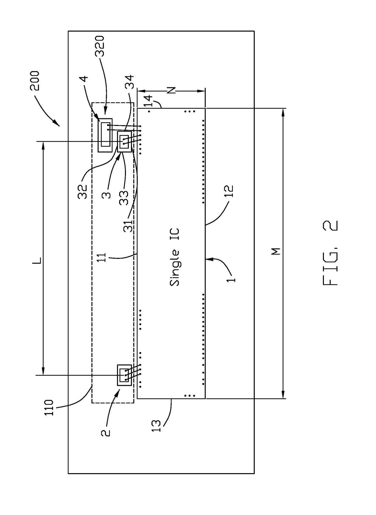
[0012]Referring to FIG. 2, a transceiver printed circuit board 200 in accordance with the present invention comprises a single IC 1, a PIN photodiode 2, a VCSEL laser 3, and a monitor pin 4. The single IC 1 has at least two different functionality from separate IC's. In the embodiment, the functionality of a transimpedance amplifier (TIA), a laser driver (LD), and a clock and data recovery (CDR) is integrated into the single IC 1. As there is no longer any intra-IC communication. In addition, the overall footprint can be reduced significantly. The single IC 1 has a first side 11, a second side 12 opposite to the first side 11, a third side 13 connecting the first side 11 and the second side 12, and a fourth side 14 opposite to the third side 13. The first side 11 is parallel to the second side 12, and the third side 13 is parallel to the fourth side 14. The length of the first side 11 and the second side 13 is larger than the length of the third side 13 and the fourth side 14, respe...

second embodiment

[0015]Referring to FIG. 3, a transceiver printed circuit board 300 in accordance with the present invention comprises a single IC 1′, the PIN photodiode 2, the VCSEL laser 3 and the monitor pin 4. Turning both the PIN photodiode 2 and the VCSEL laser 3 90° and placing the single IC 1′ in the middle of the PIN photodiode 2 and the VCSEL laser 3. The functionality of a transimpedance amplifier (TIA), a laser driver (LD) and a clock and data recovery (CDR) is integrated into the single IC 1′. As there is no longer any intra-IC communication. In addition, the overall footprint can be reduced significantly.

[0016]The single IC 1′ has a first side 11′, a second side 12′ opposite to the first side 11′, a third side 13′ connecting the first side 11 and the second side 12, and a fourth side 14′ opposite to the third side 13′. The first side 11′ is parallel to the second side 12′, and the third side 13′ is parallel to the fourth side 14′. The length of the first side 11′ and the second side 13...


PUM


Abstract

A transceiver printed circuit board (PCB) includes an integrated circuit (IC) with at least two different functionality, a photodiode and a laser. The IC has a first side, a second side opposite to the first side, a third side connecting the first side and the second side, and a fourth side opposite to the third side. The photodiode and the laser are both located in a first space beside the first side. The functionality of a transimpedance amplifier, a laser driver, and a clock and data recovery is integrated into the IC.

Description

BACKGROUND OF THE INVENTION1. Field of the Invention[0001]The present invention relates generally to a transceiver, and more particularly to a transceiver having an improving printed circuit board.2. Description of Related Arts[0002]U.S. Pat. No. 9,229,167, issued on Jan. 5, 2016, discloses a multiplexing / de-multiplexing system including a printed circuit board having a plurality of optical detectors, a plurality of transimpedance amplifier (TIA) array oriented along a direction that is parallel with the plurality of optical detectors, and a plurality of metal lines or traces. This arrangement allows the output from the TIA array to be transmitted via relatively short electrical metal lines or traces.[0003]U.S. Patent Application Publication No. 2016 / 0080090, published on Mar. 17, 2016, discloses a multi-chip module for silicon photonics including an integrated system-on-chip device. The device may be configured on a single silicon substrate member or configured on three separate si...

Claims


Application Information

Patent Timeline
IPC IPC(8): G02B6/42H04B10/40
CPCG02B6/428H04B10/40G02B6/4257G02B6/4246
Inventor ENGEL, ANDREWYU, PAULGIESSLER, KLAUSMOMTAHAN, OMIDMEADOWCROFT, DAVIDJOHN BROSNAN, MICHAEL
Owner FOXCONN INTERCONNECT TECHNOLOGY LIMITED
Why Eureka
Try Eureka