

Gate drive circuit, display panel, and driving method for the gate drive circuit
a gate drive and display panel technology, applied in the field of display technologies, can solve problems such as power consumption
- Summary
- Abstract
- Description
- Claims
- Application Information
AI Technical Summary
Benefits of technology
Problems solved by technology
Method used
Image

Examples
Embodiment Construction
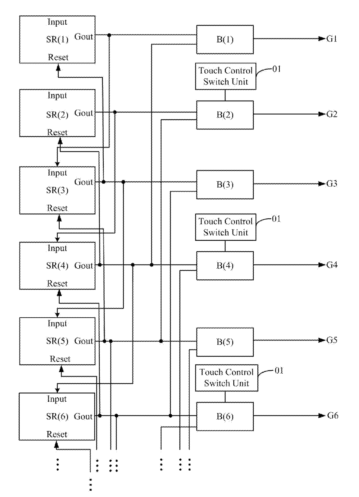
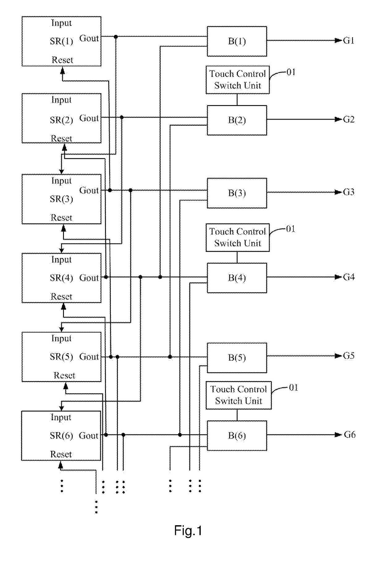
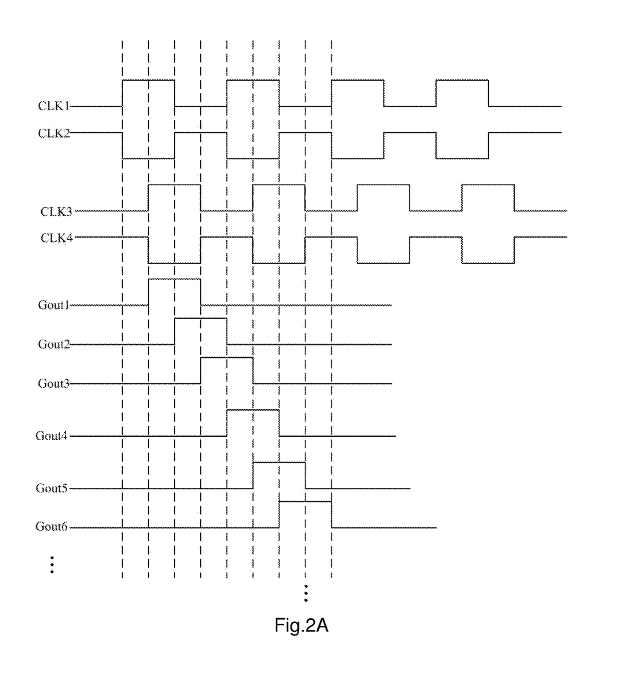
[0024]In the related art, the switching of resolution in the GOA circuit is achieved primarily by adjusting the phase relationship of clock signals via a Timer Control Register (TCON), which not only results in the delay of clock signals, resulting in poor image display, but also imposes a high requirement to the TCON, increasing the development costs of the TCON.
[0025]In view of this, embodiments of the present disclosure provide a gate drive circuit, a display panel and a driving method for the gate drive circuit, and the GOA circuit can realize the switching of resolution without modifying a TCON, thereby reducing the power consumption of the display panel.
[0026]In order to make the objects, technical solutions, and advantages of the embodiments of the present disclosure more apparent, the technical solutions according to the embodiments of the present disclosure will be described below clearly and fully with reference to the drawings in the embodiments of the present disclosure,...
PUM
 Abstract
Description
Claims
Application Information