Optical imaging device

a technology of optical imaging and optical slits, applied in the field of optical slits, can solve the problems of difficult integration of photo-detectors, in the same pixel, pin diodes, etc., and achieve the effect of improving the accuracy of image acquisition and reducing the difficulty of insertion

Active Publication Date: 2018-09-20
IDEMIA IDENTITY & SECURITY FRANCE +2
View PDF0 Cites 10 Cited by
  • Summary
  • Abstract
  • Description
  • Claims
  • Application Information

AI Technical Summary

Benefits of technology

[0017]Advantageously, the optical medium may correspond to a glass plate of a display screen. At least one part of the light sources of the pixels of this screen may form the light sources of the imaging device (not all of the light sources of the screen are necessarily used to produce the different image acquisitions). With this imaging device, it is not necessary to carry out a thinning of the glass plate at the location of the array of photo-detectors because the imaging device functions perfectly with, as optical medium, a glass corresponding to a standard protective glass of a screen. In addition, the presence of the thick optical medium does not cause loss of precision in the captured image because said optical medium forms part of the imaging device and does not perturb its operation.
[0018]Moreover, the resolution of the final image obtained of the element to image is greater than the resolution with which the array of photo-detectors is produced due to the fact that an optical magnification is naturally obtained given the path of the light rays within the optical medium (with reflection against the capture surface), and this is so without having a dedicated magnification optic present in the imaging device. For example, when the light sources and the photo-detectors are arranged in a same plane, for example produced on a same substrate, an optical magnification equal to 2 is obtained (for example, with an array of photo-detectors of resolution equal to 500 ppi, the image obtained with this imaging device is equivalent to an image that would have been captured with an initial resolution equal to 1000 ppi). An image resolution of the order of 2000 ppi or greater than 2000 ppi may also be obtained easily.
[0023]Such an imaging device proposes an architecture making it possible to obtain images of the element to image of resolution greater than or equal to 500 ppi while being compatible with production using CMOS or OLED technology.
[0027]The control and reading means, or the controller and the reader, may be configured to read, during the lighting of each of said part of the light sources, the photo-detectors located in a region of the detection surface of annular shape delimited by the reflected light rays forming, against the capture surface, the first and second limit refraction angles. For practical reasons, the control and reading means may be configured to control, on the lighting of each of said part of the light sources, the acquisition of said rays by the photo-detectors located in a region of the detection surface of square or rectangular shape including the region of the detection surface of annular shape. Thus, the reading time, or acquisition time, of the photo-detectors located in such a region of square or rectangular shape is reduced and the later digital processing of the square or rectangular images obtained with such an acquisition is then facilitated.
[0034]The light sources may comprise LEDs, and the controller and the reader may comprise CMOS transistors, or the light sources may be of OLED type, and the controller and the reader may comprise TFT transistors arranged in an interlaced manner with the array of photo-detectors. The production of the imaging device with LED technology+CMOS transistors makes it possible to attain very high resolutions. The production of the imaging device with OLED+TFT technology enables, thanks to the optical magnification obtained, the production of pixels of the imaging device with large dimensions at reduced cost, for example produced with a pitch equal to around 100 microns, and / or enhancing the resolution of the image while retaining pixels of reduced dimensions.
[0037]The control and reading means, or the controller and the reader, may be configured such that the successively switched on light sources form partial images of the element to image, that is to say having dimensions less than the total dimensions of the final image, each partially overlapping with at least one other of the partial images of the element to image, the final image next being constructed later from these different partial images. In such a configuration, the impact of one or more faulty photo-detectors is thus reduced since the overlap of the partial images makes it possible to obtain, on several of the partial images, redundant information of the element to image.

Problems solved by technology

Given the resolution required for a sensor, generally at least 500 ppi (pixels per inch), it is difficult to integrate, in a same pixel, the photo-detector (for example a PIN diode) and a light source (for example an organic light emitting diode) with their control transistor.
This necessity of having the finger positioned at a very short distance from the measuring means of the sensor is however an important drawback because it is not possible in this case to interpose between the sensor and the finger of which the print is imaged a protective element, for example a glass plate, of sufficient thickness to ensure good protection of the electronics of the sensor.
This is however very restrictive, both technologically and economically.

Method used


Image

  • Optical imaging device
  • Optical imaging device
  • Optical imaging device

Examples


first embodiment

[0031]In a first embodiment, the imaging device may advantageously be produced in the form of a CMOS electronic chip, that is to say including transistors produced using CMOS technology on a semiconductor substrate such as silicon. The light sources may in this case correspond to LEDs, advantageously produced from GaN formed beforehand on the semiconductor of the substrate.

second embodiment

[0032]In a second embodiment, the imaging device may comprise TFT transistors produced for example on a transparent substrate, for example made of glass, and light sources of OLED type.

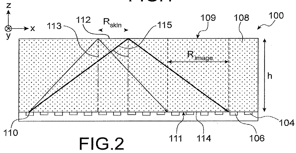
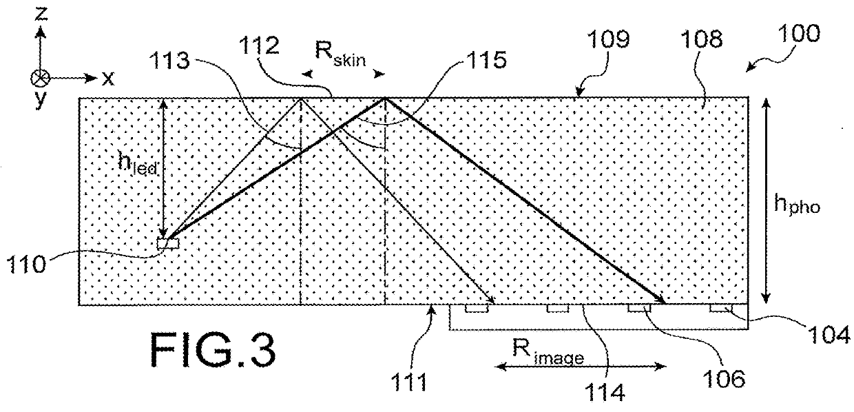
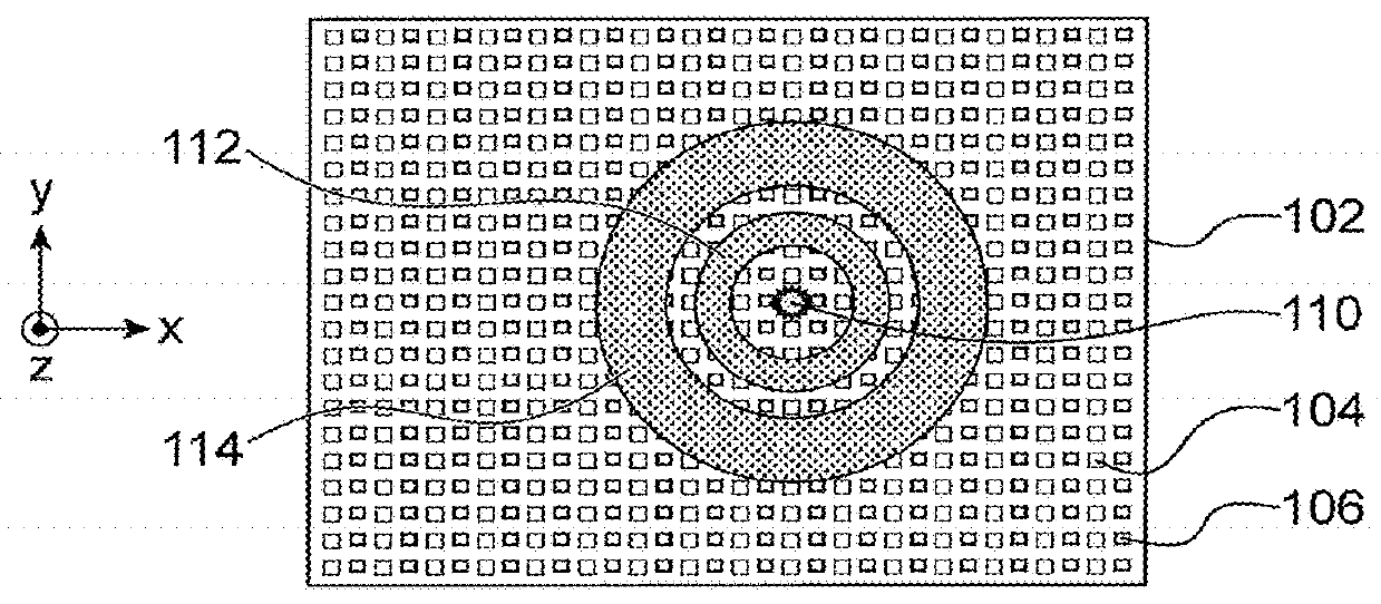
[0033]Each pixel of the display screen may comprise one of the light sources and one of the photo-detectors. In an alternative, it is however possible that certain pixels formed by the array of photo-detectors and the array of light sources does not comprise a light source (and thus uniquely a photo-detector). It is also possible that certain pixels of the display screen do not comprise photo-detectors.

[0034]The light sources may comprise LEDs, and the controller and the reader may comprise CMOS transistors, or the light sources may be of OLED type, and the controller and the reader may comprise TFT transistors arranged in an interlaced manner with the array of photo-detectors. The production of the imaging device with LED technology+CMOS transistors makes it possible to attain very high resolutions. ...


PUM


Abstract

Optical imaging device comprising:an array of substantially point light sources,an array of photo-detectors interlaced with the array of light sources,an optical medium of thickness greater than the pitch of the photo-detectors and forming capture and detection surfaces,means for successively switching on and off each of a part of the light sources and reading a part of the photo-detectors receiving rays coming from the switched on source and having undergone reflection against the detection surface while forming an angle of incidence estimated as a function of the optical medium and the element to image.

Description

TECHNICAL FIELD AND PRIOR ART[0001]The invention relates to the field of optical imaging devices, and notably that of fingerprint sensors, configured for capturing an image optically, that is to say capable of detecting light.[0002]In a fingerprint sensor that captures an image optically, it is known to use a light source of OLED (organic light emitting diode) type produced on a transparent substrate, and a photo-detector such as a diode to read the signal. Given the resolution required for a sensor, generally at least 500 ppi (pixels per inch), it is difficult to integrate, in a same pixel, the photo-detector (for example a PIN diode) and a light source (for example an organic light emitting diode) with their control transistor.[0003]Fingerprint sensors exist in which the capture of a fingerprint image is conducted in a configuration designated “in near field”, in which the finger of which the print is imaged has to be located at a short distance (of the order of the sought after r...

Claims


Application Information

Patent Timeline
Patent Type & Authority Applications(United States)
IPC IPC(8): H01L27/146G06K9/00H05B33/08H05B44/00
CPCH01L27/14609G06K9/00013H05B33/0803H01L27/14643H05B45/30G06V40/1324H01L27/14678H10K59/65G06V40/1318G06V40/1335
Inventor MAINGUET, JEAN-FRANCOISTEMPLIER, FRANCOIS
Owner IDEMIA IDENTITY & SECURITY FRANCE
Why Eureka
Try Eureka