Transfer head and transfer system for semiconductor light-emitting device and method for transferring semiconductor light-emitting device

a transfer head and light-emitting device technology, applied in the field of display devices, can solve the problems of difficult flexibility implementation, short life, and slow response time, and achieve the effects of high grip force, precise alignment control, and large area

Active Publication Date: 2018-09-27
LG ELECTRONICS INC
View PDF0 Cites 42 Cited by
  • Summary
  • Abstract
  • Description
  • Claims
  • Application Information

AI Technical Summary

Benefits of technology

[0019]In the present invention, a Johnsen rahbek type electrostatic gripper may be applied to a method of transferring a semiconductor light-emitting device by using an electrode of a transfer head and an undoped semiconductor layer of a semiconductor light-emitting device. Therefore, a method and apparatus of transferring a semiconductor light-emitting device with a higher grip force may be implemented. Also, in this case, each of a base substrate and an electrode unit is provided to have light transmissivity, and thus, precise control for alignment is possible with a field of upper view.
[0020]Moreover, by transferring a plurality of semiconductor light-emitting devices with a multi-head having light transmissivity, the present invention can have an advantage in large area and a plurality of transfer. Also, by using low-cost glass for the base substrate having light transmissivity, the manufacturing cost of a transfer head can be reduced.
[0021]Moreover, according to the present invention, it is easy that a number of semiconductor light-emitting devices are pixelized on a wafer, and then, are selectively transferred to a substrate with precision.
[0022]Moreover, by using an electrostatic plate having a simple structure without a complicated mesa structure, the present invention realizes the low manufacturing cost and a high yield rate. Furthermore, due to the simple structure, the present invention has control precision, and large-area transfer is possible.
[0023]Moreover, the present invention transfers a plurality of semiconductor light-emitting devices by using a transfer head having light transmissivity, and thus, can have an advantage in large area and a plurality of transfer.
[0024]Moreover, according to the present invention, horizontality and step heights of pickup heads and a donor substrate may be aligned without using a sensor and a transfer mechanism.

Problems solved by technology

However, in LCD devices, a response time is not fast, and it is difficult to implement flexibility.
In AMOLEDs, lifetime is short, a yield rate is not good, and a flexible degree is weak.
Examples of such a transfer method include a method using a PDMS stamp type transfer head or an electrostatic gripper, etc., but all of such methods have a problem which alignment is difficult.
Moreover, the methods have a problem where the manufacturing cost is high, and a yield rate is low.
However, the actuator which rotates and is transferred along the multi-axis are based on input values of various sensors (sensors recognizing an image, a distance, etc.), but have a problem where the input values are inaccurate and a problem where it is unable to adjust accurate horizontality.
Also, horizontal alignment is made between the transfer wafer and the receiver wafer, but in a case where there is a slope locally or there is a height difference locally, it is difficult to pick up a micro-device.

Method used


Image

  • Transfer head and transfer system for semiconductor light-emitting device and method for transferring semiconductor light-emitting device
  • Transfer head and transfer system for semiconductor light-emitting device and method for transferring semiconductor light-emitting device
  • Transfer head and transfer system for semiconductor light-emitting device and method for transferring semiconductor light-emitting device

Examples


third embodiment

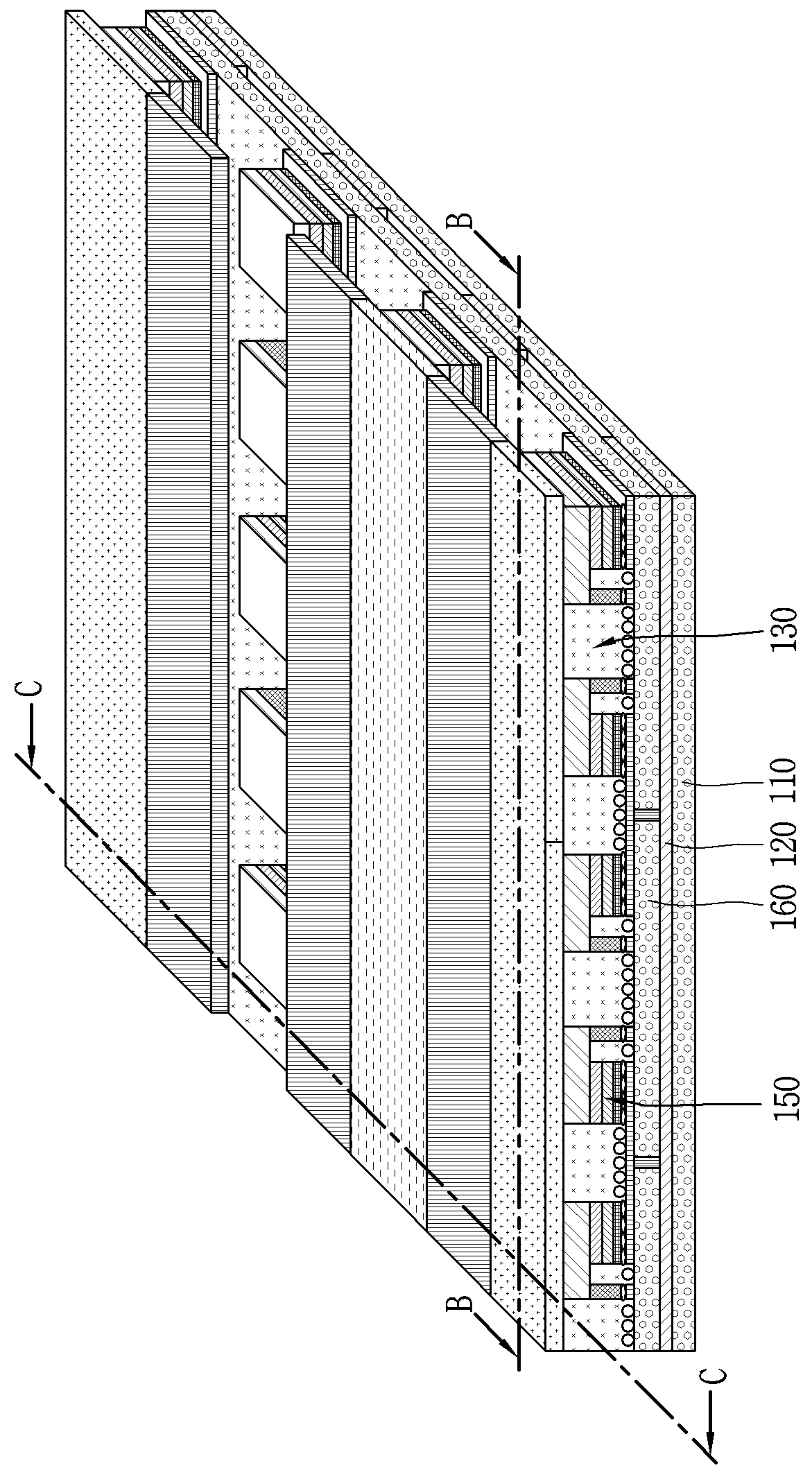
[0352]Referring to FIG. 28, a head holder 8120 of a third embodiment includes a through hole 8122 for enhancing flexibility. The through hole 8122 is formed in a support surface 8128 of the head holder 8120. In detail, the through hole 8122 is formed to pass through the head holder 8120 in a direction intersecting the support surface 8128 of the head holder 8120.

[0353]For example, as illustrated in FIG. 28, the through hole 8122 is provided in plurality, and the plurality of through holes 8122 are disposed in a line shape in the support surface 8128 of the head holder 8120. The line-shaped through holes 8122 are arranged at certain pitches. The line-shaped through holes 8122 may have a matrix type intersecting one another.

[0354]Preferably, the head holder 8120 includes a plurality of holder blocks B which are disposed on a horizontal surface and are spaced apart from each other. The plurality of holder blocks B may be defined by the line-shaped through hole 8122.

[0355]At least one p...

seventh embodiment

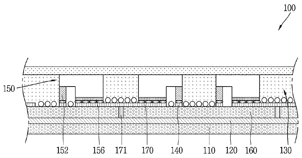
[0378]In the present embodiment, the head holder 8220 is formed in a plat shape and supports a plurality of pickup heads 8130. In this case, a head holder 8220 of a seventh embodiment may use material which is higher than that of the head holder 8220 of the preceding embodiment. For example, the head holder 8220 of an embodiment uses a resin material having flexibility.

[0379]The spacer 8140 structurally supports the head holder 8220. The spacer 8140 is located between the head holder 8220 and the substrate 8110. The spacer 8140 is located in a portion of a space between the head holder 8220 and the substrate 8110.

[0380]A shape of the spacer 8140 is deformed by a movement of each of a plurality of pickup heads 8130, and thus, the spacer 8140 provides a degree of freedom to the head holder 8220. When the spacer 8140 is deformed, a slope and a curvature of the head holder 8220 are deformed, thereby providing a degree of freedom to the pickup head 8130.

[0381]In detail, a level of each o...


PUM


Abstract

The present invention relates to a display device and, more particularly, to a transfer head for a semiconductor light-emitting device applied to the display device and a method for transferring a semiconductor light-emitting device. The transfer head for a semiconductor light-emitting device, according to the present invention, comprises: a base substrate; and an electrode unit disposed on the base substrate to generate an electrostatic force by charging an un-doped semiconductor layer of the semiconductor light-emitting device with electric charges, wherein the base substrate and the electrode unit are formed of light-transmitting materials so that at least a part of the semiconductor light-emitting device is viewable through the base substrate and the electrode unit in sequence.

Description

TECHNICAL FIELD[0001]The present invention relates to a display device using a semiconductor light-emitting device, and more particularly, to a transfer head and a transfer system for semiconductor light-emitting devices and a method for transferring semiconductor light-emitting devices.BACKGROUND ART[0002]Recently, in display technology field, display devices having good characteristics such as thinness and flexibility are being developed. On the other hand, examples of currently commercialized main display devices include liquid crystal display (LCD) devices and active matrix organic light-emitting diodes (AMOLEDs).[0003]However, in LCD devices, a response time is not fast, and it is difficult to implement flexibility. In AMOLEDs, lifetime is short, a yield rate is not good, and a flexible degree is weak.[0004]Light-emitting diodes (LEDs) are well known semiconductor light-emitting devices which convert a current into light, and red LEDs using a GaAsP compound semiconductor have b...

Claims


Application Information

Patent Timeline
Patent Type & Authority Applications(United States)
IPC IPC(8): H01L25/075H01L33/62H01L33/22
CPCH01L25/0753H01L33/62H01L33/22H01L2933/0066H01L2933/0033H01L21/6835H01L33/0095H01L2221/68354H01L21/677
Inventor MOON, SUNGHYUNCHANG, YOUNGHAKJEON, JINAKIM, SEONHOOYEE, YOUNGJOOYUH, HWANKUK
Owner LG ELECTRONICS INC
Why Eureka
Try Eureka