Pixel Arrangement Mode Sharing Blue Light Light Emitting Layer and Organic Electroluminescent Device

Active Publication Date: 2018-10-04
KUNSHAN NEW FLAT PANEL DISPLAY TECH CENT +1
View PDF1 Cites 8 Cited by
  • Summary
  • Abstract
  • Description
  • Claims
  • Application Information

AI Technical Summary

Benefits of technology

[0005]In consideration of this, the present invention is intended to solve the technical problem that the pixel arrangement mode in prior art cannot reach a high PPI resolution and its device preparation process still needs to use high precision masks and the production process is complicated, by providing a pixel arrangement with a shared blu

Problems solved by technology

But the highest precision of a precision metal mask is limited by processing levels, which causes that the resolution of organic electroluminescent display devices is difficult to increase.
In another aspect, because the precision mask has a high precision and every light emitting area needs aligning and adjustment, while each time of adjustment causes the finished product ratio of display devices to decrease, the device cost is increased

Method used


Image

  • Pixel Arrangement Mode Sharing Blue Light Light Emitting Layer and Organic Electroluminescent Device
  • Pixel Arrangement Mode Sharing Blue Light Light Emitting Layer and Organic Electroluminescent Device
  • Pixel Arrangement Mode Sharing Blue Light Light Emitting Layer and Organic Electroluminescent Device

Examples


embodiment 1

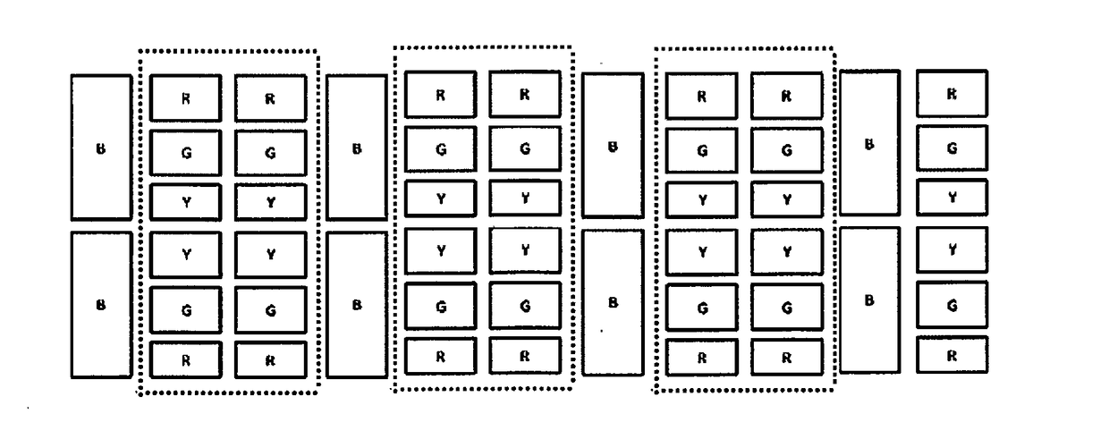
[0065]As shown in FIG. 3, a pixel arrangement with a shared blue light emitting layer comprises m rows and n columns of first pixel units, wherein, the first pixel units are blue light sub-pixels, m is a non-zero natural number, n is a natural number larger than or equal to 2, two columns of second pixel units are arranged between neighboring first pixel units, each of the second pixel units comprises a red light sub-pixel, and a green light sub-pixel and a yellow light sub-pixel that are arranged in a juxtaposed manner. Every dotted line block in FIG. 3 includes two rows and two columns of second pixel units.

[0066]The red light sub-pixel, the green light sub-pixel and the yellow light sub-pixel in the second pixel unit have completely or partially overlapping projections in a row direction.

[0067]The red light sub-pixel, the green light sub-pixel and the yellow light sub-pixel in the second pixel unit have no overlapping projection on the blue light sub-pixel. Every two neighboring ...

embodiment 2

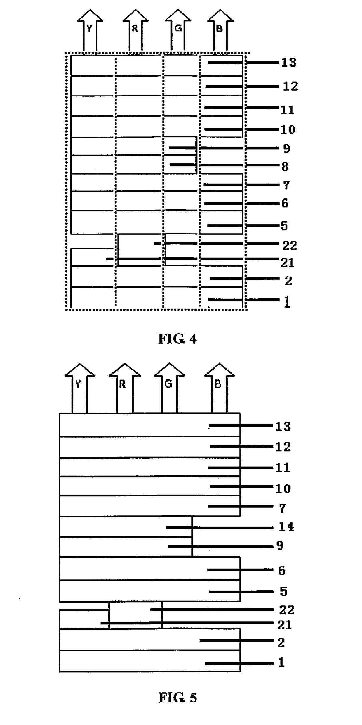
[0068]As shown in FIG. 4, this embodiment provides an organic electroluminescent device having the pixel arrangement according to Embodiment 1, comprising a substrate (not shown), with a first electrode layer, a plurality of light emitting unit layers and a second electrode layer 12 formed in sequence on the substrate, as well as an optical coupling layer 13 upon the second electrode layer 12, wherein the first electrode layer comprises a first conducting layer 1 and a second conducting layer 2 arranged in sequence upon the substrate, and the light emitting unit layers comprise a hole injection layer 5, a hole transport layer 6, a light emitting layer, an electron transport layer 10 and an electron injection layer 11 arranged in sequence upon second conducting layer 2.

[0069]The light emitting layer comprises a blue light emitting layer 7 and a yellow light emitting layer 9 that are stacked with a blocking layer interposed between them. The blue light emitting layer 7 covers the hole...

embodiment 3

[0082]As shown in FIG. 5, in this embodiment, the organic electroluminescent device having a pixel arrangement with a shared blue light emitting layer has similar structure as that of Embodiment 2, except that the positions of the blue light emitting layer 7 and the yellow light emitting layer 9 within the light emitting layer are switched, and that the blocking layer adopts a hole blocking layer 14. That is, the yellow light emitting layer 9 covers part of the hole transport layer 6, the blocking layer covers the yellow light emitting layer 9, part of the blue light emitting layer 7 covers the blocking layer, and the blocking layer is a hole blocking layer 14.

[0083]The preparation method of an organic electroluminescent device having a pixel arrangement with a shared blue light emitting layer according to this embodiment comprises the following steps:[0084]S1, evaporation coating a first conducting layer 1 and a second conducting layer 2 in sequence upon a substrate by using an ope...


PUM


Abstract

Disclosed is a pixel arrangement with a shared blue light emitting layer (7), comprising m rows and n columns of first pixel units, the first pixel units are blue light sub-pixels (B), m is a non-zero natural number, n is a natural number larger than or equal to 2, wherein, two columns of second pixel units are arranged between neighboring first pixel units, each of the second pixel units comprises a red light sub-pixel (R), a green light sub-pixel (G) and a yellow light sub-pixel (Y) that are arranged in a juxtaposed manner. By properly modifying the pixel arrangement of the device configuration, light emitting in four colors can be achieved by using only two or less sets of low precision masks in the preparation process, so that the resolution is increased with reduced cost, and as compared to conventional pixel arrangement, the PPI can be doubled, reaching 600 PPI.

Description

TECHNICAL FIELD[0001]The present invention relates to the technical field of organic electroluminescent devices, and in particular relates to a pixel arrangement with a shared blue light emitting layer and an organic electroluminescent device having the pixel arrangement.BACKGROUND[0002]An organic electroluminescent display device (OLED) usually includes a plurality of pixels, and each pixel is composed of several light emitting areas. Currently, one widely used solution in small and medium sized devices is forming a pixel with three sub-pixels of red, green and blue. In order to obtain high pixel resolution, the three types of light emitting areas of red, green and blue need to be evaporation coated respectively by using high precision masks, and therefore three sets of precision metal masks are needed. But the highest precision of a precision metal mask is limited by processing levels, which causes that the resolution of organic electroluminescent display devices is difficult to i...

Claims


Application Information

Patent Timeline
IPC IPC(8): H01L27/32H01L51/50H01L51/52H01L51/56H01L51/00
CPCH01L27/3218H01L27/3213H01L27/322H01L51/504H01L51/5056H01L51/5072H01L51/5088H01L51/5092H01L51/5096H01L51/5265H01L51/56H01L51/001H01L2251/558H01L51/0067H01L51/0052H01L51/006H01L51/0058H01L51/0072H01L51/0059H01L51/0085H01L51/0081H10K59/351H10K59/353H10K59/38H10K50/131H10K50/18H10K50/852H10K2102/351H10K59/35H10K50/13H10K50/14H10K50/17H10K50/15H10K50/16H10K50/171H10K71/00H10K71/164H10K85/324H10K85/342H10K85/615H10K85/626H10K85/631H10K85/633H10K85/654H10K85/6572
Inventor LI, WEIWEILIU, SONGHUANG, XIUQILUO, ZHIZHONG
Owner KUNSHAN NEW FLAT PANEL DISPLAY TECH CENT
Why Eureka
Try Eureka