Gip circuit and driving method therefor, and flat panel display device

a technology of gip circuit and driving method, which is applied in the direction of digital storage, semiconductor devices, instruments, etc., can solve the problems of screen operation failure, abnormal display of images subsequent, and incorrect display of strips across the screen, so as to improve driving, avoid ripple effect, and simple structur

Active Publication Date: 2018-11-08
KUNSHAN NEW FLAT PANEL DISPLAY TECH CENT
View PDF0 Cites 5 Cited by
  • Summary
  • Abstract
  • Description
  • Claims
  • Application Information

AI Technical Summary

Benefits of technology

The present invention provides a simple GIP circuit that can produce signals that can be easily turned off from high levels to low levels. This circuit includes a control signal that remains high, and a transistor that causes the electric potential of a node to drop. As a result, the output of the circuit produces a high level signal. This GIP circuit is useful in driving a flat panel display, as it helps improve display quality and avoids ripple.

Problems solved by technology

Once a GIP signal from a certain cascade is incorrect, the corresponding pixels cannot be gated, leading to display anomalies on a display screen of the flat panel display 100 such as operation failure of the screen, incorrect display in a strip across the screen, or abnormal display of images subsequent to correct display of them.
However, the drive units in the conventional GIP circuit 10 are usually circuits of a so-called 10T3C structure which is complex and incorporates a relatively large number of thin-film transistors (TFTs).
Additionally, the GIP signals generated by the drive units cannot be neatly pulled down from a high level to a low level.
This may cause ripples which are detrimental to the display quality of the flat panel display device.

Method used


Image

  • Gip circuit and driving method therefor, and flat panel display device
  • Gip circuit and driving method therefor, and flat panel display device
  • Gip circuit and driving method therefor, and flat panel display device

Examples


Embodiment Construction

[0032]The GIP circuit, driving method and flat panel display device proposed in the present invention will be described below in greater detail with reference to particular embodiments which are to be read in conjunction with the accompanying drawings. Features and advantages of the invention will be more apparent from the following detailed description. It is noted that the figures are provided in a very simplified form not necessarily presented to scale, with the only intention to facilitate convenience and clarity in explaining the embodiments.

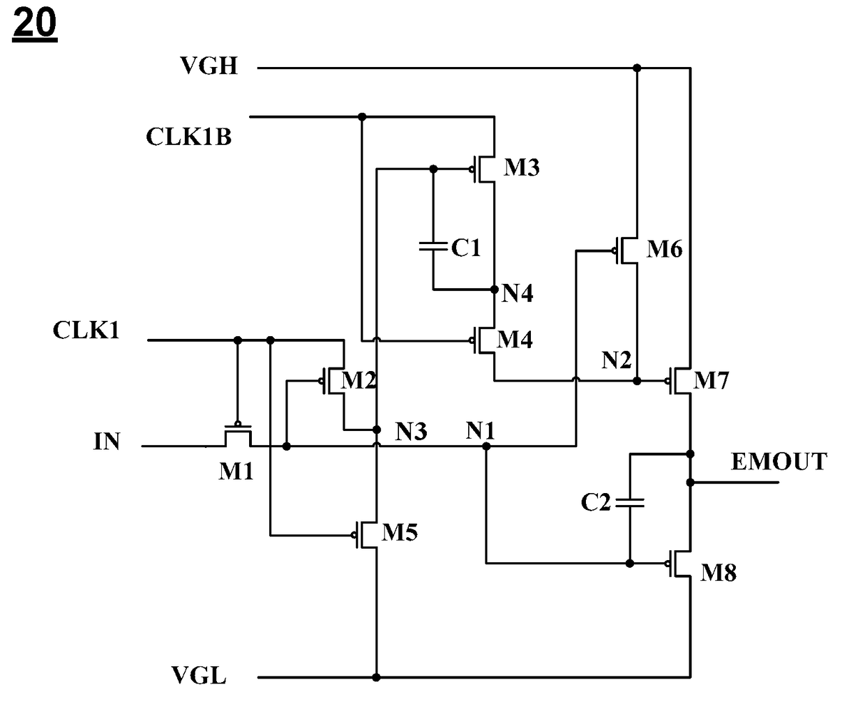
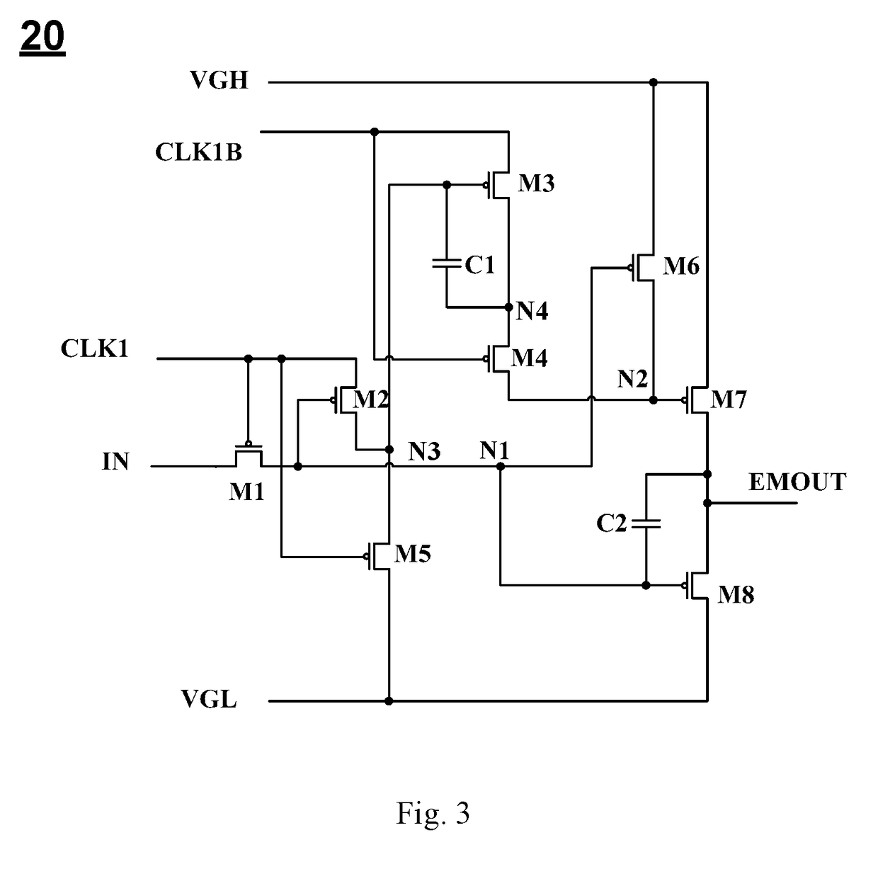
[0033]Referring to FIG. 3, a GIP circuit according to an embodiment of the present invention is schematically illustrated. As shown in FIG. 3, the GIP circuit includes a plurality of cascaded drive units 20, each being connected to a drive control line IN, a first gate line VGH, a second gate line VGL, a first clock signal line CLK1 and a second clock signal line CLK1B and including first to eighth transistors M1-M8, a first capacitor C1 an...


PUM


Abstract

A GIP circuit, a method for driving the GIP circuit and a flat panel display device incorporating the GIP circuit. The GIP circuit is simple in structure and is capable of producing GIP signals that can be neatly pulled from a high level down to a low level. This allows better driving, avoids ripples and achieves higher display quality of the flat panel display device.

Description

TECHNICAL FIELD[0001]The present invention relates to the field of flat panel displays and, in particular, to a gate-in-panel (GIP) circuit, a method for driving the GIP circuit and a flat panel display device.BACKGROUND[0002]Rapid development and application of the information technology, wireless mobile communications and information appliances in recent years have been increasing our dependence on electronics and have brought about prosperity for various display technologies and devices. Flat panel display devices are finding extensive use for their complete flatness, lightweight, slimness, higher energy efficiency and other advantages.[0003]At present, in order to reduce the manufacturing cost of flat panel display devices and allow narrow bezels thereof, the gate-in-panel (GIP) technology is usually used to directly integrate gate drive circuits (i.e., GIP circuits) into flat display panels. Such a gate drive circuit includes multiple drive units for generating GIP signals at m...

Claims


Application Information

Patent Timeline
IPC IPC(8): G09G3/20H01L27/12
CPCG09G3/20H01L27/124G09G2310/08G09G2300/0809G09G2310/0289G09G2300/0408G02F1/13454G09G3/2092G09G3/2096G09G2310/0267G09G2310/0286G09G3/3677G09G3/3266G09G2230/00G09G2320/0209G11C19/28G09G2300/0819G09G3/035G09G2310/0278
Inventor YANG, NANZHU, HUIHU, SIMINGZHANG, TINGTINGSONG, YANQIN
Owner KUNSHAN NEW FLAT PANEL DISPLAY TECH CENT
Why Eureka
Try Eureka