Semiconductor device having metal gate

a metal gate and semiconductor technology, applied in the direction of semiconductor devices, basic electric elements, electrical appliances, etc., can solve the problems of reducing the gate capacitance, lowering the driving force of the device, and reducing the trench area, so as to facilitate the enhancement of the efficiency of the nmos, reduce the difficulty in filling the conductive layer, and reduce the trench area

Active Publication Date: 2018-12-13
UNITED MICROELECTRONICS CORP
View PDF5 Cites 13 Cited by
  • Summary
  • Abstract
  • Description
  • Claims
  • Application Information

AI Technical Summary

Benefits of technology

[0007]One feature of the invention is that after the top barrier layer is completed, an additional silicon formation layer is additionally formed on the top barrier layer, and a planarization process is then performed to control the depth of the gate trench, and the aspect ratio of the trench can be reduced. Thereby the difficulty in filling the conductive layer is decreased. In addition, in one embodiment of the present invention, the silicon generating layer reacts with the top barrier layer to form a titanium silicide nitride layer which facilitates the enhancement of the efficiency of the NMOS.

Problems solved by technology

With the trend towards scaling down the size of semiconductor devices, conventional poly-silicon gates face problems such as boron penetration and unavoidable depletion effect leading to inferior performance.
Because of these problems, the equivalent thickness of the gate dielectric layer increases, reducing the gate capacitance, and lowering a driving force of the devices.

Method used


Image

  • Semiconductor device having metal gate
  • Semiconductor device having metal gate
  • Semiconductor device having metal gate

Examples


Embodiment Construction

[0010]To provide a better understanding of the present invention to users skilled in the technology of the present invention, preferred embodiments are detailed as follows. The preferred embodiments of the present invention are illustrated in the accompanying drawings with numbered elements to clarify the contents and effects to be achieved.

[0011]Please note that the figures are only for illustration and the figures may not be to scale. The scale may be further modified according to different design considerations. When referring to the words “up” or “down” that describe the relationship between components in the text, it is well known in the art and should be clearly understood that these words refer to relative positions that can be inverted to obtain a similar structure, and these structures should therefore not be precluded from the scope of the claims in the present invention.

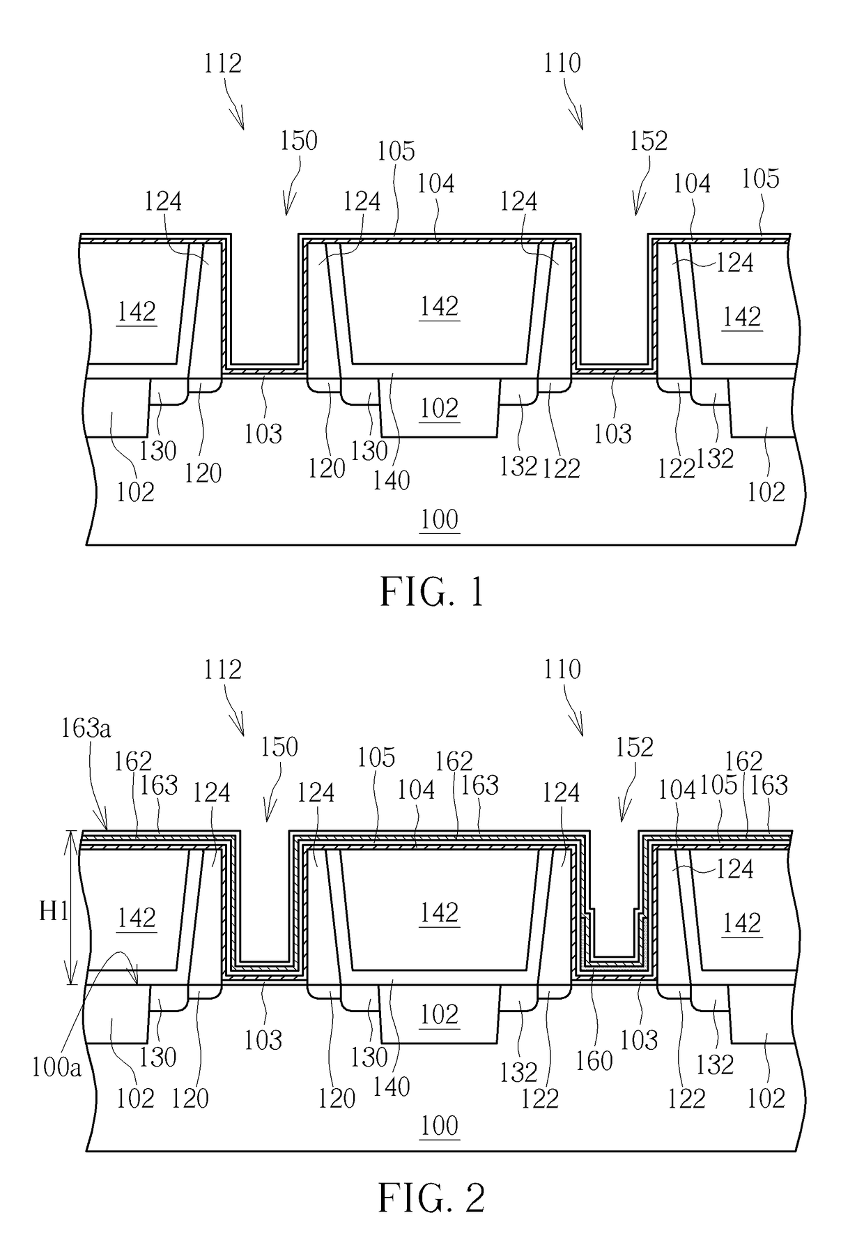
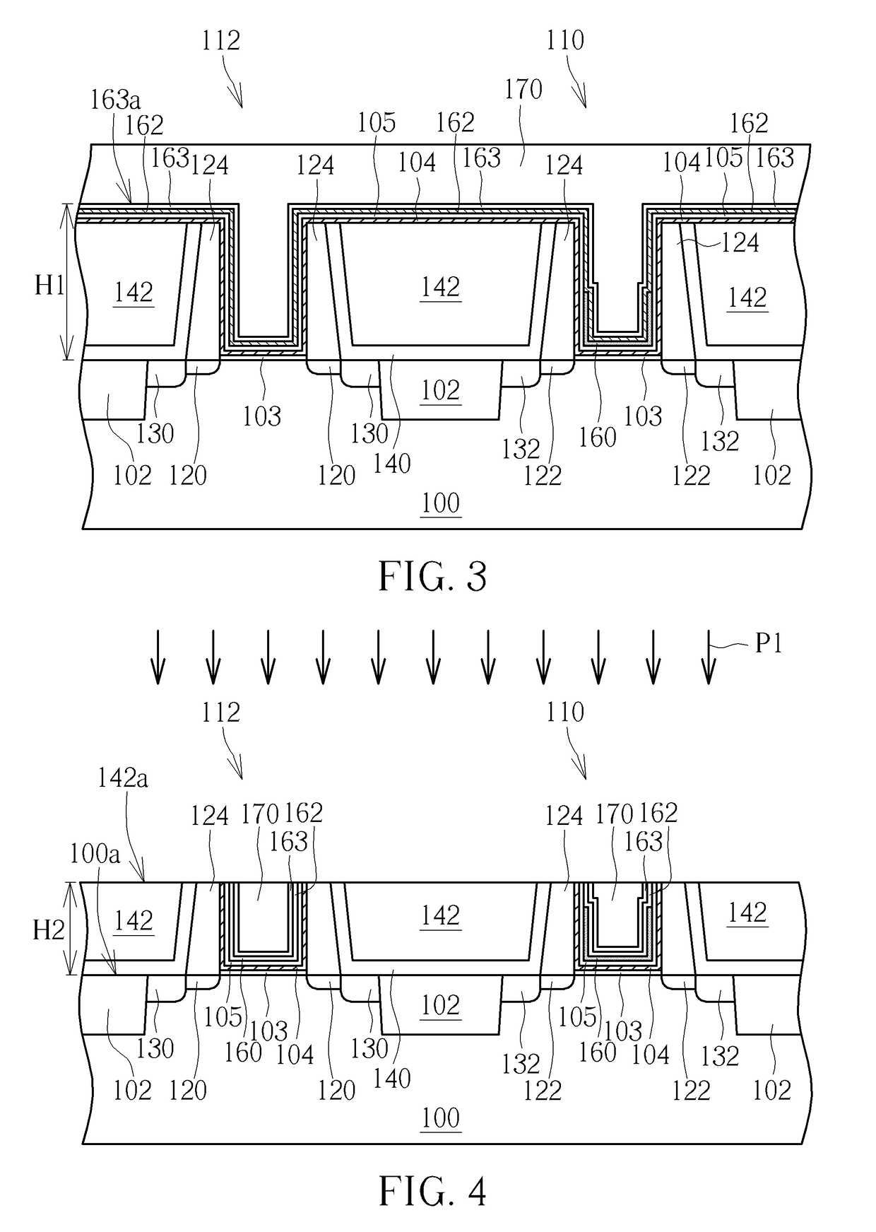
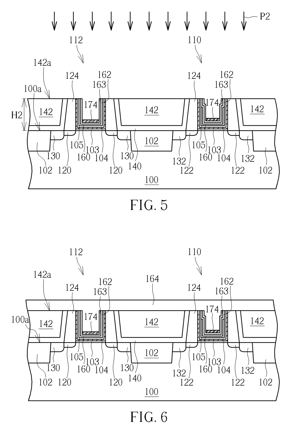
[0012]Please refer to FIGS. 1-7, which are drawings illustrating a manufacturing method for semiconduct...


PUM


Abstract

The present invention provides a method of manufacturing a gate stack structure. The method comprises providing a substrate. A dielectric layer is then formed on the substrate and a gate trench is formed in the dielectric layer. A bottom barrier layer, a first work function metal layer and a top barrier layer are formed in the gate trench in sequence. Afterwards, a silicon formation layer is formed on the top barrier layer and filling the gate trench. A planarization process is performed, to remove a portion of the silicon formation layer, a portion of the bottom barrier layer, a portion of the first work function metal layer, and a portion of the top barrier layer. Next, the remaining silicon formation layer is removed completely, and a conductive layer is filled in the gate trench.

Description

BACKGROUND OF THE INVENTION1. Field of the Invention[0001]The invention relates to a manufacturing method for a semiconductor device having a metal gate, and more particularly, to a manufacturing method for a semiconductor device having a metal gate integrated with the gate last process and the high-k last process.2. Description of the Prior Art[0002]Poly-silicon is conventionally used as a gate electrode in semiconductor devices, such as metal-oxide-semiconductors (MOS). With the trend towards scaling down the size of semiconductor devices, conventional poly-silicon gates face problems such as boron penetration and unavoidable depletion effect leading to inferior performance. Because of these problems, the equivalent thickness of the gate dielectric layer increases, reducing the gate capacitance, and lowering a driving force of the devices. Therefore, work function metals that are suitable for use as high dielectric constant (high-k) gate dielectric layers are employed to replace t...

Claims


Application Information

Patent Timeline
Patent Type & Authority Applications(United States)
IPC IPC(8): H01L29/49H01L21/28H01L21/02
CPCH01L29/4975H01L21/02074H01L21/28088H01L21/823842H01L29/4966H01L29/513H01L29/517H01L29/66545
Inventor CHIANG, CHUN-TINGLEE, CHI-JULIN, CHIH-WEISU, BO-YUWU, YEN-LIANGCHANG, WEN-TSUNGYANG, JUI-MINGCHANG, I-FAN
Owner UNITED MICROELECTRONICS CORP
Why Eureka
Try Eureka