Radiation detector element and imager comprising an assembly of radiation detector elements

a radiation detector and element technology, applied in the direction of diodes, radiation controlled devices, semiconductor devices, etc., can solve the problems of not having the same electrical resistance to the passage of the detector element, the performance of the detector element is not optimized, and the resistance of the detector element is often significan

Active Publication Date: 2018-12-27
THALES SA +1
View PDF5 Cites 1 Cited by
  • Summary
  • Abstract
  • Description
  • Claims
  • Application Information

AI Technical Summary

Problems solved by technology

However, such detector elements often have a significant resistance to the passage of the current.
As a result, when an imager comprises several detector elements sharing a shared electric contact, the detector elements do not all have the same electrical resistance to the passage of the current.
The performance of the detector element is therefore not optimized.

Method used


Image

  • Radiation detector element and imager comprising an assembly of radiation detector elements
  • Radiation detector element and imager comprising an assembly of radiation detector elements
  • Radiation detector element and imager comprising an assembly of radiation detector elements

Examples


Embodiment Construction

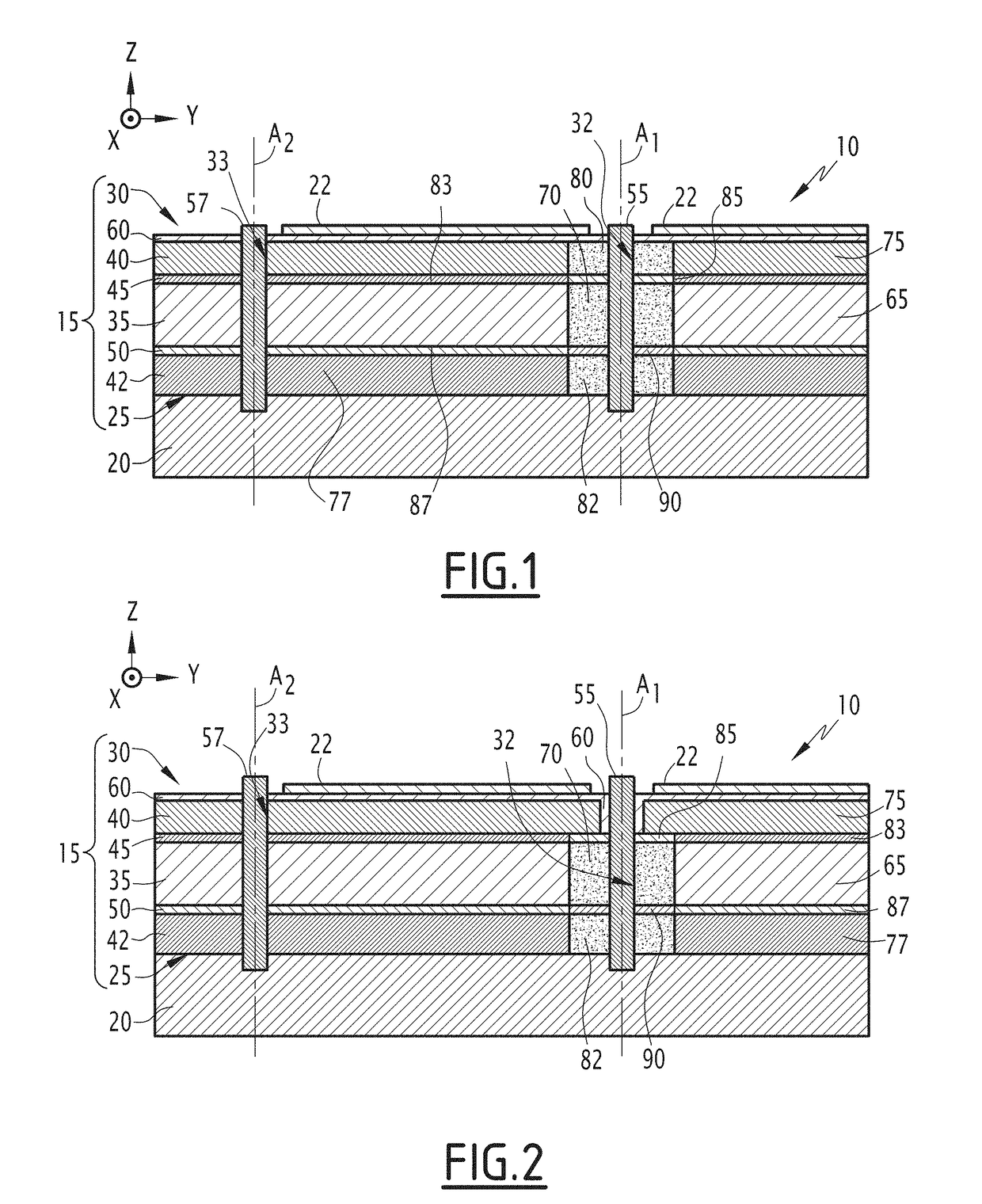
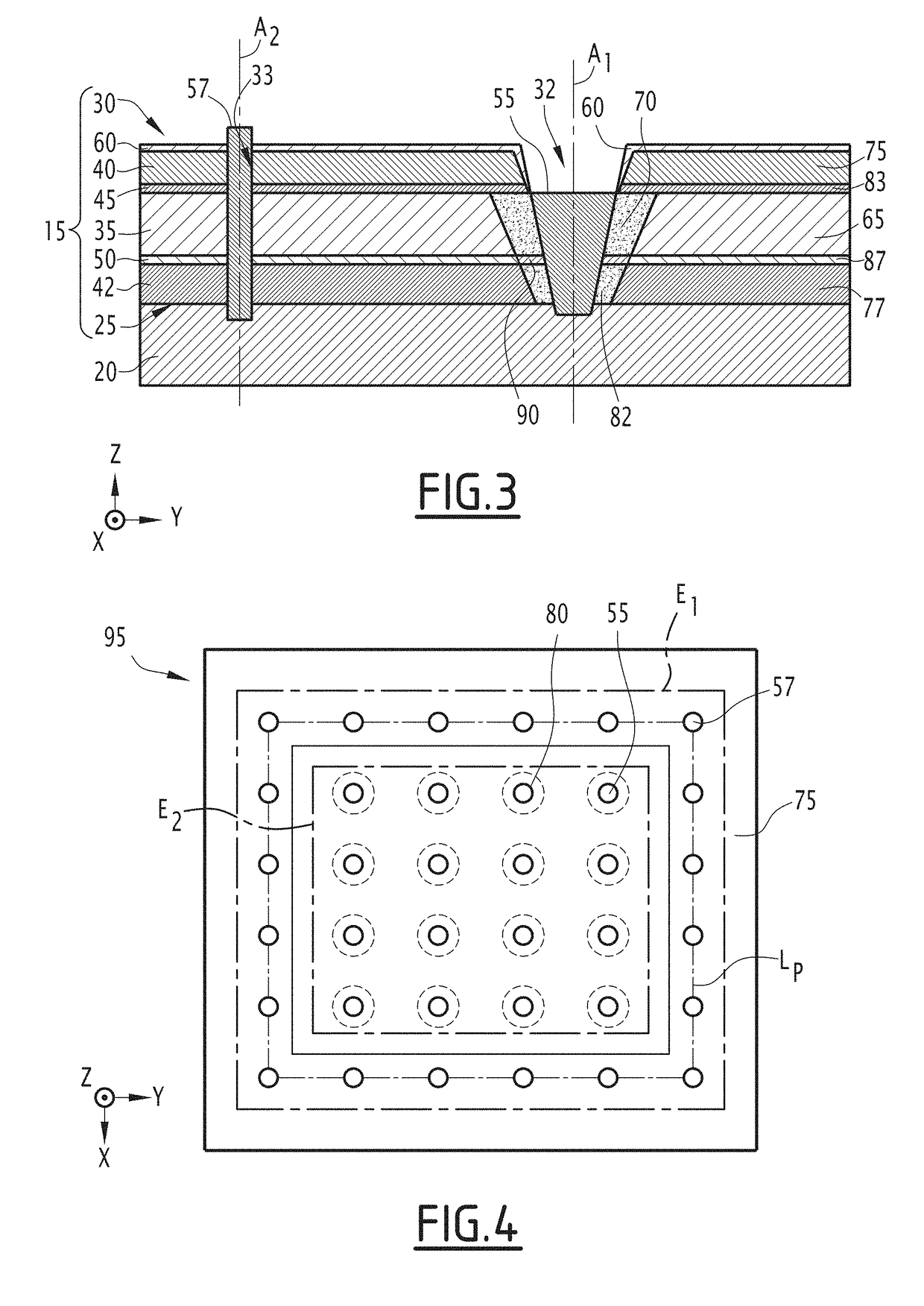
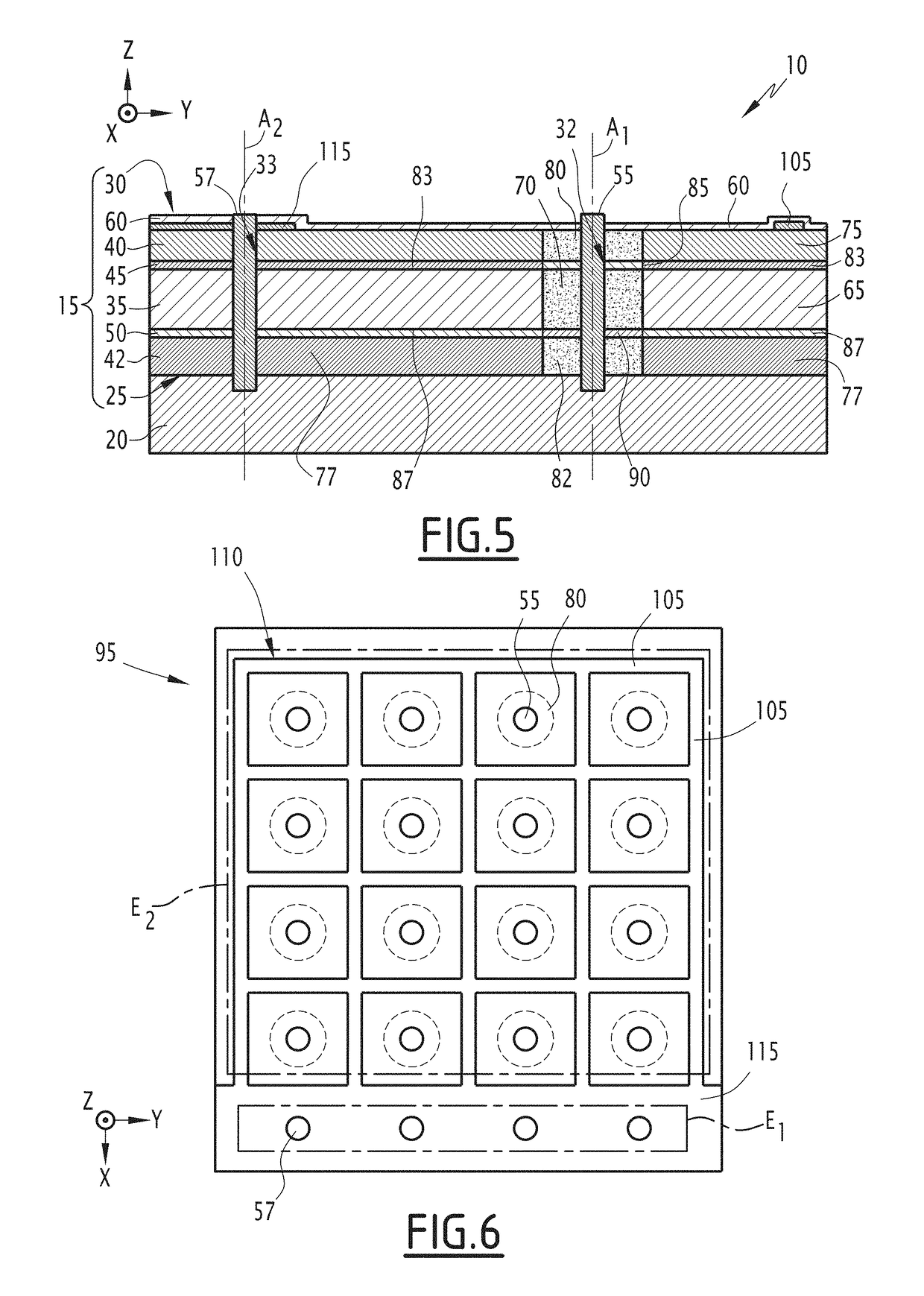
[0038]A first example radiation detector element 10 is shown in FIG. 1.

[0039]The detector element 10 is able to generate an electrical signal S when the detector element 10 absorbs radiation R.

[0040]The radiation R comprises at least one electromagnetic wave Oe.

[0041]The electromagnetic wave Oe has at least an energy E and an amplitude A.

[0042]The energy E is defined as the product of the Planck constant h and the frequency f of the electromagnetic wave Oe in a vacuum.

[0043]The amplitude A is defined as the Euclidian norm of the electric field of the electromagnetic wave Oe.

[0044]The electrical signal S is an electric current. For example, the electrical signal S is an electric current proportional to the amplitude A of the electromagnetic wave Oe.

[0045]The radiation detector element 10 comprises a stack 15 of superimposed layers and a reading circuit 20. Optionally, as is the case for the example of FIG. 1, the detector element 10 also comprises a filtering layer 22.

[0046]The stack...


PUM


Abstract

Disclosed is a radiation detector element including a stack of layers superimposed in a stacking direction, the stack having a first face and a second face and including a radiation-absorbing layer consisting of a first semiconductor material having a first band gap value and at least one barrier layer consisting of a second semiconductor material having a second band gap value, the second band gap value being strictly greater than the first band gap value. The stack further delimits a primary hole traversing each of the layers of the stack, the primary hole receiving at least part of a primary electrode. The barrier layer includes a first conducting zone having a free carrier density greater than or equal to 1.1017/cm−3.

Description

FIELD OF THE INVENTION[0001]The present invention relates to a radiation detector element, as well as an imager comprising a set of radiation detector elements.BACKGROUND OF THE INVENTION[0002]Generally, electromagnetic radiation detector devices comprise a matrix of individual radiation detector elements. Such radiation detector devices, also called “imagers”, further comprise a reading circuit able to receive an electrical signal from each radiation detector element. The imager is able to reconstitute a two-dimensional image from electrical signals provided by each detector element.[0003]The radiation detector elements used are frequently made from semi-conductive materials. For example, silicon radiation detector elements of the CCD (Charge-Coupled Device) or CMOS (Complementary Metal-Oxide-Semiconductor) type are used in digital cameras capable of detecting visible electromagnetic radiation. For other radiation ranges, such as infrared radiation, other types of radiation detecto...

Claims


Application Information

Patent Timeline
Patent Type & Authority Applications(United States)
IPC IPC(8): H01L27/146
CPCH01L27/14638H01L27/14636H01L27/14603H01L27/14643H01L27/14601H01L27/14649H01L27/14652H01L27/14694
Inventor LEGOFF, FLORIANREVERCHON, JEAN-LUCKAZMIERSKI, CHRISTOPHEDECOBERT, JEAN
Owner THALES SA
Why Eureka
Try Eureka