Two-dimensional electrostrictive field effect transistor (2d-efet)

a two-dimensional electrostrictive field and transistor technology, applied in the direction of basic electric elements, electrical apparatus, semiconductor devices, etc., can solve the problems of increasing the power density at the same rate, increasing static and leakage power densities at a much faster rate, and power/heat dissipation, henceforth, becoming the main problem. , to achieve the effect of reducing the band gap of two-dimensional layered materials

Active Publication Date: 2018-12-27
PENN STATE RES FOUND
View PDF3 Cites 20 Cited by
  • Summary
  • Abstract
  • Description
  • Claims
  • Application Information

AI Technical Summary

Benefits of technology

[0014]Yet another embodiment of the method may have additional steps of forming a second gate, wherein the channel is disposed between the gate and the second gate. The second gate has a second column of an electrostricti...

Problems solved by technology

This inevitably led to increase in the power density at the same rate as the integration density.
The actual scenario worsened by the non-scaling factors, which escalated the static and leakage power densities at a much faster rate.
Power/heat dissipation, henceforth, became the main problem for the high performance microprocessors.
Today, in 2016, even the dimension scaling seems extremely challenging beyond 10 nm gate length (LG...

Method used


Image

  • Two-dimensional electrostrictive field effect transistor (2d-efet)
  • Two-dimensional electrostrictive field effect transistor (2d-efet)
  • Two-dimensional electrostrictive field effect transistor (2d-efet)

Examples


embodiment 600

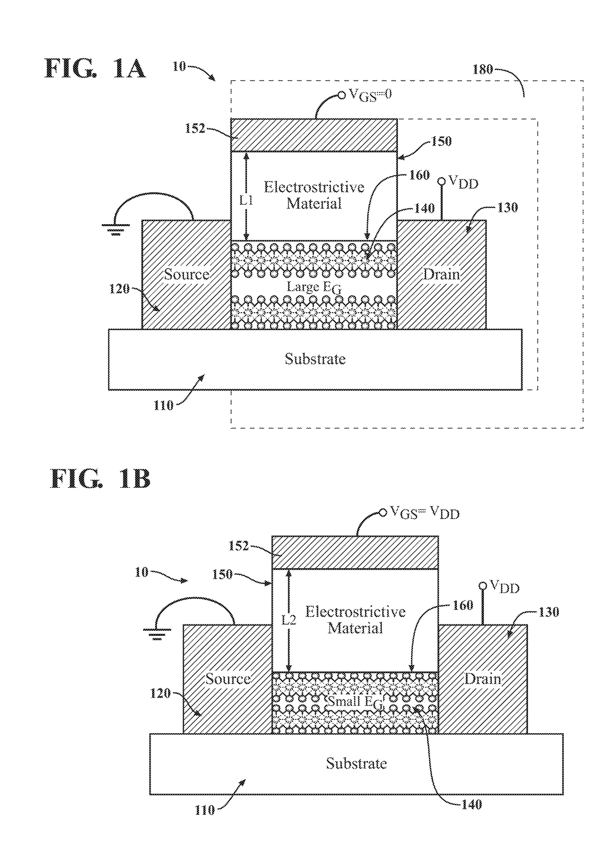
[0071]FIG. 6 is a cross-sectional block diagram of a 2D-EFET according to another embodiment of the present invention. The embodiment 600 shown in the FIG. 6 has four terminals i.e. source 610, drain 620, gate 630, back gate 640, and a capping layer 690. The 2D-EFET 600 may be manufactured by depositing a layer of the back gate 640 on a substrate 650. Consecutive layers of a gate 630, and a dielectric 670 may be deposited on the back gate 640. The gate 630 includes a column of electrostrictive material 660 that is deposited on the back gate 640. The source 610, drain 620, and at least one layer of 2D material 680 may be provided on the dielectric layer 670. The 2D material 680 comprises a first surface 605 toward the capping layer 690 and a second surface 615 toward the dielectric 670. According to a non-limiting embodiment, the resulting assembly of the electrostrictive material 660, gate 630, dielectric 670, source 610, drain 620, and at least one layer of 2D material 680 may be e...

embodiment 800

[0075]FIG. 8 is a cross-sectional block diagram of a 2D-EFET according to another embodiment of the present invention. The embodiment 800 shown in the FIG. 8 has four terminals i.e. source 818, drain 810, first gate 814, second gate 804, and a capping layer 802. The 2D-FET 800 may be manufactured by depositing a layer of the first gate 814 on a substrate 816. Consecutive layers of a 2D-material 808, and the second gate 804 may be deposited on the first gate 814. The first gate 814 and the second gate 804 respectively include columns of electrostrictive material 812, and electrostrictive material 806 that are deposited toward the 2D-material 808. The source 818 and drain 810 are connected to the columns of electrostrictive material 812 and 806 toward an opposing side away from the first gate 814 and second gate 804, respectively. According to a non-limiting embodiment, the resulting assembly of electrostrictive material 806, electrostrictive material 812, first gate 814, second gate ...


PUM


Abstract

A device and method for manufacturing a two-dimensional electrostrictive field effect transistor having a substrate, a source, a drain, and a channel disposed between the source and the drain. The channel is a two-dimensional layered material and a gate proximate the channel. The gate has a column of an electrostrictive or piezoelectric or ferroelectric material, wherein an electrical input to the gate produces an elongation of the column that applies a force or mechanical stress on the channel and reduces a bandgap of two-dimensional material such that the two-dimensional electrostrictive field effect transistor operates with a subthreshold slope that is less than 60 mV/decade.

Description

CROSS-REFERENCE TO RELATED APPLICATIONS[0001]This application claims priority from Provisional Application No. 62 / 523,520 filed Jun. 22, 2017, the entire content of which is incorporated herein by reference.GOVERNMENT SUPPORT[0002]This invention was made with government support under Grant No. ECCS1640020, awarded by National Science Foundation. The Government has certain rights in the invention.FIELD OF THE INVENTION[0003]The present invention is related to a device and method for manufacturing a two-dimensional electrostrictive field effect transistor having a substrate, a gate, a source, a drain, and a channel disposed between the source and the drain. The channel is a two-dimensional layered material. The gate has a column of an electrostrictive or piezoelectric or ferroelectric material, wherein an electrical input to the gate produces an elongation of the column that applies a force or stress on the channel and reduces the bandgap of the two-dimensional material. The change in...

Claims


Application Information

Patent Timeline
IPC IPC(8): H01L29/84H01L29/66H01L29/51H01L29/778H01L29/24H01L29/76
CPCH01L29/84H01L29/66969H01L29/516H01L29/778H01L29/24H01L29/7606H01L29/66977H01L29/1033
Inventor DAS, SAPTARSHI
Owner PENN STATE RES FOUND
Why Eureka
Try Eureka