Monolithically Integrated InGaN/GaN Quantum Nanowire Devices

a quantum nanowire and monolithic technology, applied in the direction of semiconductor devices, basic electric elements, electrical equipment, etc., can solve the problems of limited lifetime of organic materials, low efficiency and brightness, and relatively expensive manufacturing process

Active Publication Date: 2018-12-27
RGT UNIV OF MICHIGAN
View PDF5 Cites 14 Cited by
  • Summary
  • Abstract
  • Description
  • Claims
  • Application Information

AI Technical Summary

Benefits of technology

[0011]As the inventors have found, with the structural and optical properties of InGaN / GaN quantum layers depended upon nanowire diameter, a unique monolithically integrated fabrication may form InGaN / GaN nanowire light emitting diode (LED) devices that have a collective emission wavelength tunable across an entire spectral range (e.g., across a visible spectral range). By controlling the diameters of the nanowire structures and the percentage composition of In, Ga, and N in the respective InGaN / GaN quantum layers of the nanowires, it is now possible to engineer a cluster that emits over a tunable wide spectral range, by selecting the emitting wavelengths of each individual nanowire. Moreover, the monolithically integrated fabrication allows for precise control over the spacing between nanowire structures during fabrication, where that spacing, for the first time, allows for not only nanowires of different diameters, but also for the precise control over composition of elements in the quantum active regions, which otherwise would make it impossible to form a cluster having a wide emission spectral range.

Problems solved by technology

The challenges of organic light emitting diodes (OLEDs) for these applications include limited lifetime of organic materials, relatively expensive manufacturing process, low efficiency and brightness, and poor stability.
Moreover, it has remained difficult to achieve micro-scale or nano-scale devices using organic materials.
It has also remained difficult to achieve efficient deep green and red emission using GaN-based quantum well LEDs.
Additionally, there is no established technology to spatially vary Indium (In) compositions in quantum wells to achieve multicolor emission on the same substrate.
Furthermore, it has been shown that multicolor emission can be achieved from InGaN nanowire arrays monolithically integrated on a single chip.
To date, however, little is known about the mechanism on how to controllably vary the alloy compositions at the single nanowire level without changing the global growth parameters.
The monolithic integration of multicolor, single nanowire LEDs on the same chip has thus remained elusive.
It is desirable, and extremely challenging, to be able to fabricate a semiconductor-based light-emitting photonic device that has all the following attributes.

Method used


Image

  • Monolithically Integrated InGaN/GaN Quantum Nanowire Devices
  • Monolithically Integrated InGaN/GaN Quantum Nanowire Devices
  • Monolithically Integrated InGaN/GaN Quantum Nanowire Devices

Examples


Embodiment Construction

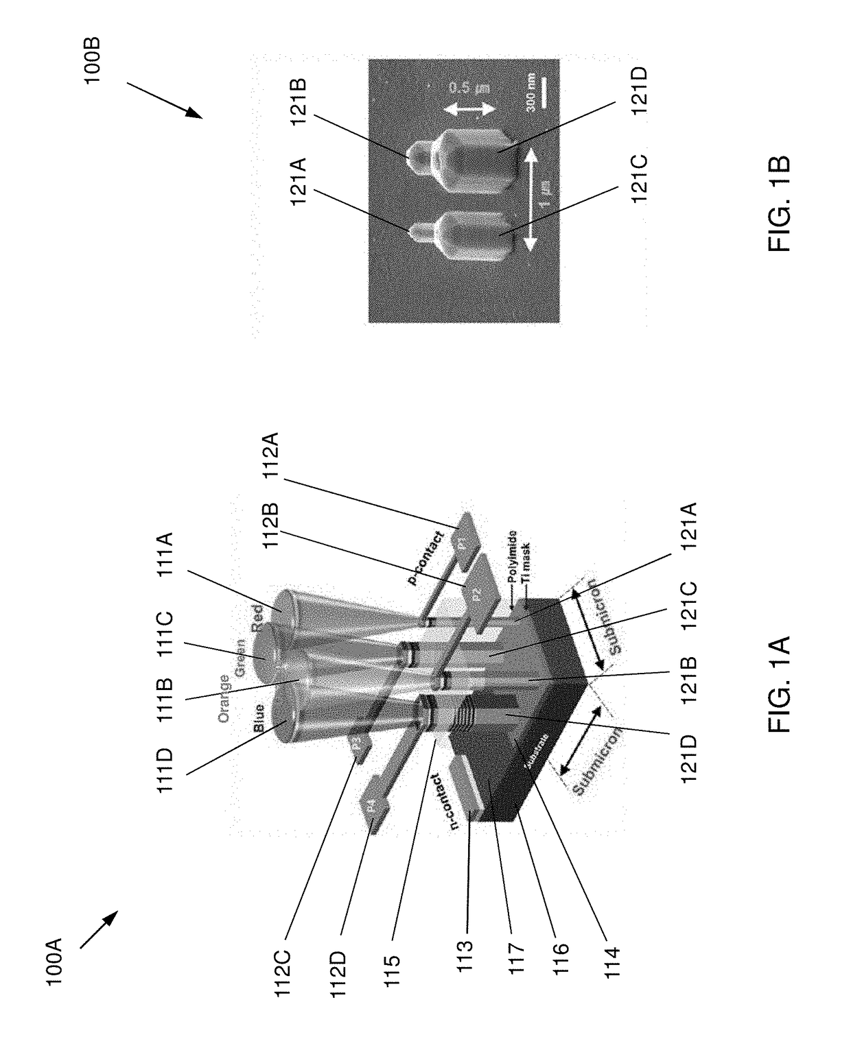
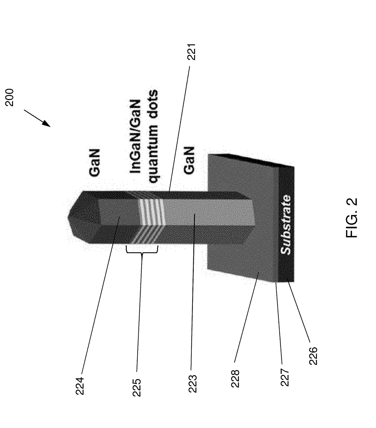
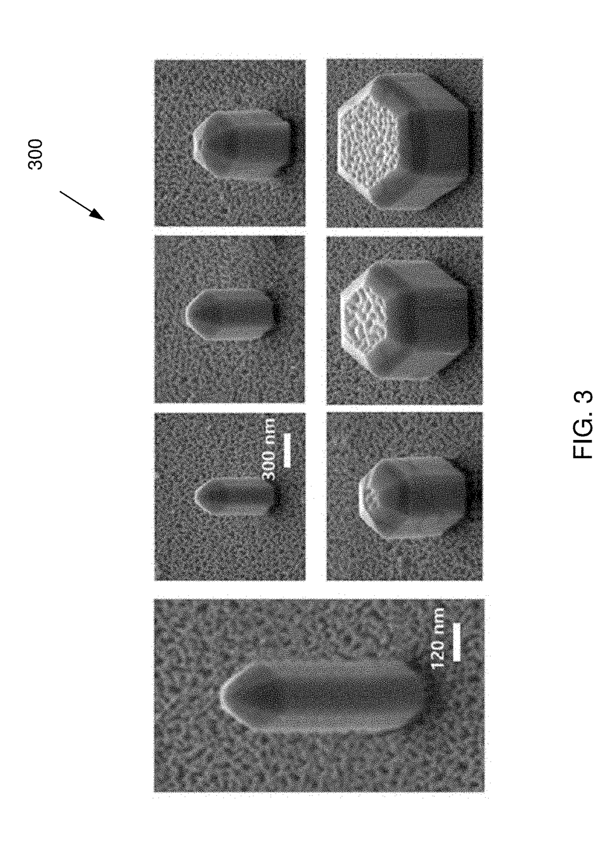
[0038]The present techniques include methods of fabricating solid-state semiconductor nanowires and devices formed of the same. The nanowires are novel InGaN / GaN quantum layer active region nanowires. These nanowires may be fabricated as photon emitting devices, such as light emitting diodes (LEDs), or as photodetectors that absorb light at specified wavelengths. Techniques herein further describe tuning the wavelength of the photon output of nanowires by fabricating them at different diameter. Indeed, using a novel monolithically integrated fabrication process, a cluster of nanowires can be formed together into a single, repeatable cluster of nanowires each emitting at different, tuned wavelength. The fabrication techniques are able to form these clusters having nanowires of different diameters, each capable of emitting at a different peak wavelength, such that the entire cluster is able to provide an output over a range of frequencies, such as over the entire visible spectrum. Eac...


PUM


Abstract

InGaN / GaN quantum layer nanowire light emitting diodes are fabricated into a single cluster capable of exhibiting a wide spectral output range. The nanowires having InGaN / GaN quantum layers formed of quantum dots are tuned to different output wavelengths using different nanowire diameters, for example, to achieve a full spectral output range covering the entire visible spectrum for display applications. The entire cluster is formed using a monolithically integrated fabrication technique that employs a single-step selective area epitaxy growth.

Description

FIELD OF THE DISCLOSURE[0001]The present disclosure relates to solid-state semiconductor devices and, more specifically, to semiconductor-based quantum nanowire devices formed of InGaN / GaN quantum structures.BACKGROUND[0002]The background description provided herein is for the purpose of generally presenting the context of the disclosure. Work of the presently named inventors, to the extent it is described in this background section, as well as aspects of the description that may not otherwise qualify as prior art at the time of filing, are neither expressly nor impliedly admitted as prior art against the present disclosure.[0003]Driven by the need for smaller size, reduced power consumption, and enhanced efficiency and functionality, future ultrahigh resolution display technologies require the development of submicron-scale, high-efficiency, multicolor light sources monolithically integrated on a single chip. The challenges of organic light emitting diodes (OLEDs) for these applica...

Claims


Application Information

Patent Timeline
Patent Type & Authority Applications(United States)
IPC IPC(8): H01L33/06H01L33/32H01L33/00H01L33/24H01L27/15
CPCH01L33/06H01L33/32H01L33/0075H01L33/24H01L27/15H01L33/0025H01L27/156H01L33/007H01L33/08H01L33/18H01L33/20H01L33/38H01L33/62H01L2933/0016
Inventor MI, ZETIANRA, YONG-HOWANG, RENJIE
Owner RGT UNIV OF MICHIGAN
Why Eureka
Try Eureka