Housing for simple assembly of an ewod device

a technology of ewod and assembly, which is applied in the field of droplet microfluidic devices and their construction, can solve the problems of inconvenient use, significant disadvantages of mother-glass assembly, and high production costs, and achieve the effect of facilitating device construction and assembly, reducing production costs, and simplifying the assembly and construction of ewod or am-ewod devices

Active Publication Date: 2019-01-17
SHARP LIFE SCI EU LTD
View PDF0 Cites 0 Cited by
  • Summary
  • Abstract
  • Description
  • Claims
  • Application Information

AI Technical Summary

Benefits of technology

[0016]The manner of assembly and construction of an EWOD or AM-EWOD device needs to be simplified while maintaining high overall performance of the resultant device. Accordingly, the present disclosure describes an enhanced device construction of an EWOD or AM-EWOD device and related assembly methods that facilitate device construction and assembly to provide a low-cost and simplified manner to assemble individual EWOD devices. Multiple devices, therefore, can be assembled efficiently without the disadvantages associated with conventional mother-glass level assembly.

Problems solved by technology

The configuration and related assembly of structures such as those described in U.S. Pat. No. 9,011,662, which is typical of the conventional art, results in a substantial number of complicated and expensive production techniques.
However, there are also significant disadvantages of mother-glass assembly.
This specialized equipment is expensive and may not be suitable for certain facilities depending on size.
The manufacturing process for creating a patterned hydrophobic layer at mother-glass scale is complex.
Conventional housings and related manufacturing processes for EWOD devices, therefore, remain deficient.

Method used


Image

  • Housing for simple assembly of an ewod device
  • Housing for simple assembly of an ewod device
  • Housing for simple assembly of an ewod device

Examples


Embodiment Construction

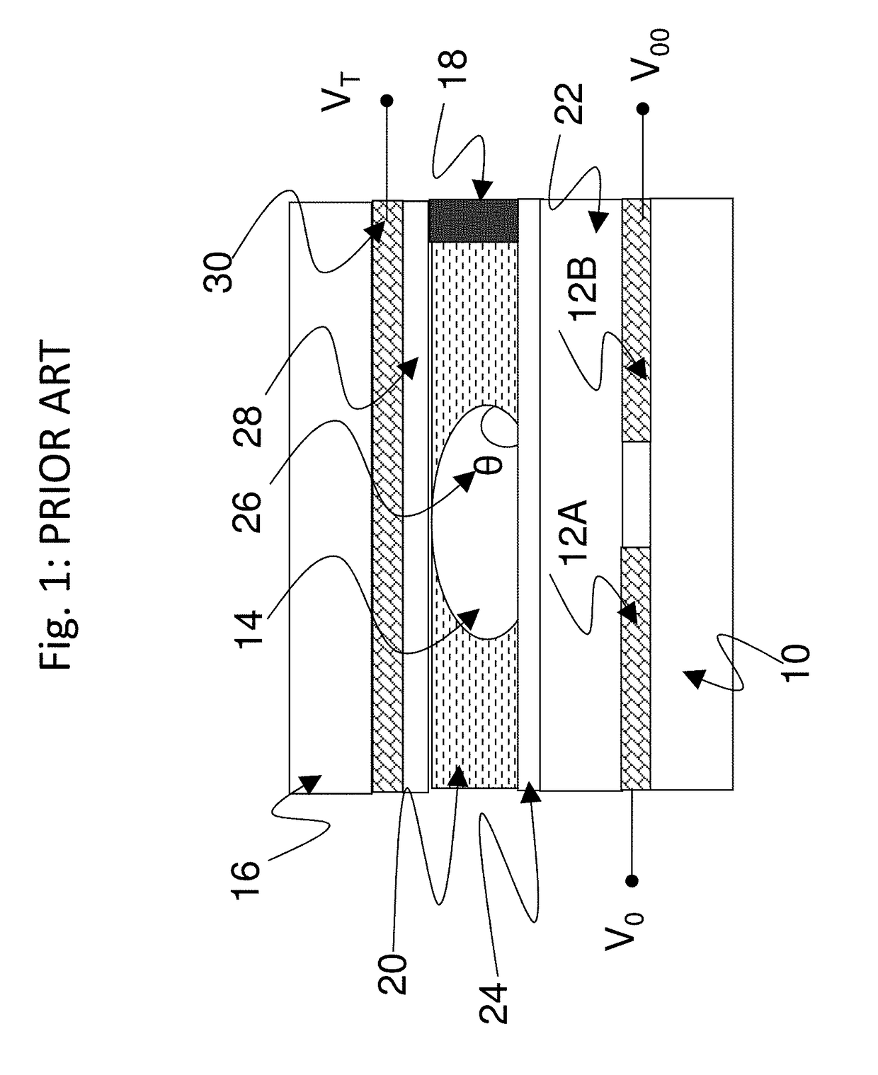
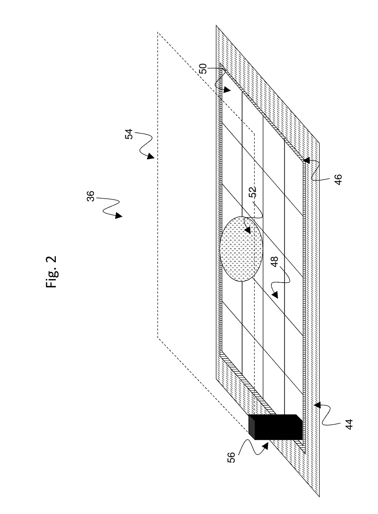
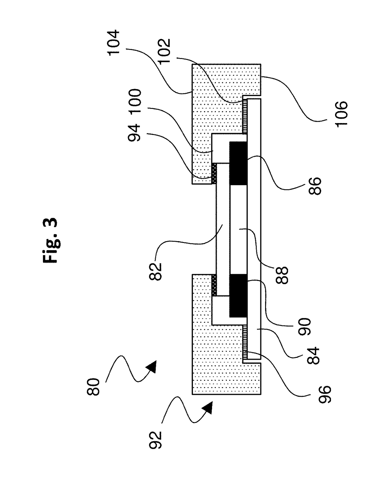
[0044]Embodiments of the present invention will now be described with reference to the drawings, wherein like reference numerals are used to refer to like elements throughout. It will be understood that the figures are not necessarily to scale.

[0045]FIG. 3 is a drawing depicting a side cross-section view of an exemplary EWOD device 80 in accordance with embodiments of the present invention. The EWOD device 80 includes a first or upper substrate assembly 82 and a second or lower substrate assembly 84 separated by a spacer 86. For simplicity of illustration of pertinent features, the individual layers of the EWOD device components are omitted. Accordingly, the first and second substrate assemblies may include the associated glass substrate layers, insulating layers, electrode layers, and related structures that form the EWOD device as are known in the art. Typically, the second (lower) substrate assembly 84 constitutes the TFT substrate that would include the thin film electronics, wi...


PUM

PropertyMeasurementUnit
electro-wetting voltagesaaaaaaaaaa
viscosityaaaaaaaaaa
electric fieldaaaaaaaaaa

Abstract

An EWOD device includes a first substrate assembly and a second substrate assembly; wherein one of said substrate assemblies includes electrowetting electrodes, and the first substrate assembly and the second substrate assembly are spaced apart to define a channel between the substrate assemblies; and a housing for receiving the first substrate assembly and the second substrate assembly, the housing comprising an alignment feature for locating at least one of the first and second substrate assemblies within the housing. The device further includes a fixing feature for fixing the first and second substrate assemblies within the housing. The second substrate assembly is located within the housing such that the second substrate assembly is an outer component of the EWOD device. The device further may include a spacer that spaces apart the first substrate assembly from the second substrate assembly to define the channel between the first and second substrate assemblies.

Description

TECHNICAL FIELD[0001]The present invention relates to droplet microfluidic devices and their construction, and more specifically to Active Matrix Electro-wetting-On-Dielectric (AM-EWOD) devices, including housing structures for simplified assembly and configurations of such devices.BACKGROUND ART[0002]Electrowetting on dielectric (EWOD) is a well-known technique for manipulating droplets of fluid by the application of an electric field. Active Matrix EWOD (AM-EWOD) refers to implementation of EWOD in an active matrix array incorporating transistors, for example by using thin film transistors (TFTs). It is thus a candidate technology for digital microfluidics for lab-on-a-chip technology. An introduction to the basic principles of the technology can be found in “Digital microfluidics: is a true lab-on-a-chip possible?”, R. B. Fair, Microfluid Nanofluid (2007) 3:245-281).[0003]FIG. 1 shows a part of a conventional EWOD device in cross section. The device includes a lower substrate 10,...

Claims


Application Information

Patent Timeline
Patent Type & Authority Applications(United States)
IPC IPC(8): B01L3/00G02B26/00G01N27/447
CPCB01L3/502792B01L3/50273G02B26/005G01N27/44791G01N27/44704B01L2300/0645B01L2300/0816B01L2300/089B01L2300/165B01L2400/0427
Inventor PARRY-JONES, LESLEY ANNEWALTON, EMMA JAYNE
Owner SHARP LIFE SCI EU LTD
Why Eureka
Try Eureka