Apparatus and method for soldering a plurality of chips using a flash lamp and a mask

a technology of flash lamps and masks, applied in the field of soldering, can solve the problems of incompatible reflow soldering, low decomposition temperature of low-cost flexible foils, time-consuming process using large in-line ovens, etc., and achieves the effect of preventing overheating, reducing the number of chips, and relatively fast heating

Active Publication Date: 2019-01-24
NEDERLANDSE ORG VOOR TOEGEPAST-NATUURWETENSCHAPPELIJK ONDERZOEK (TNO)
View PDF0 Cites 5 Cited by
  • Summary
  • Abstract
  • Description
  • Claims
  • Application Information

AI Technical Summary

Benefits of technology

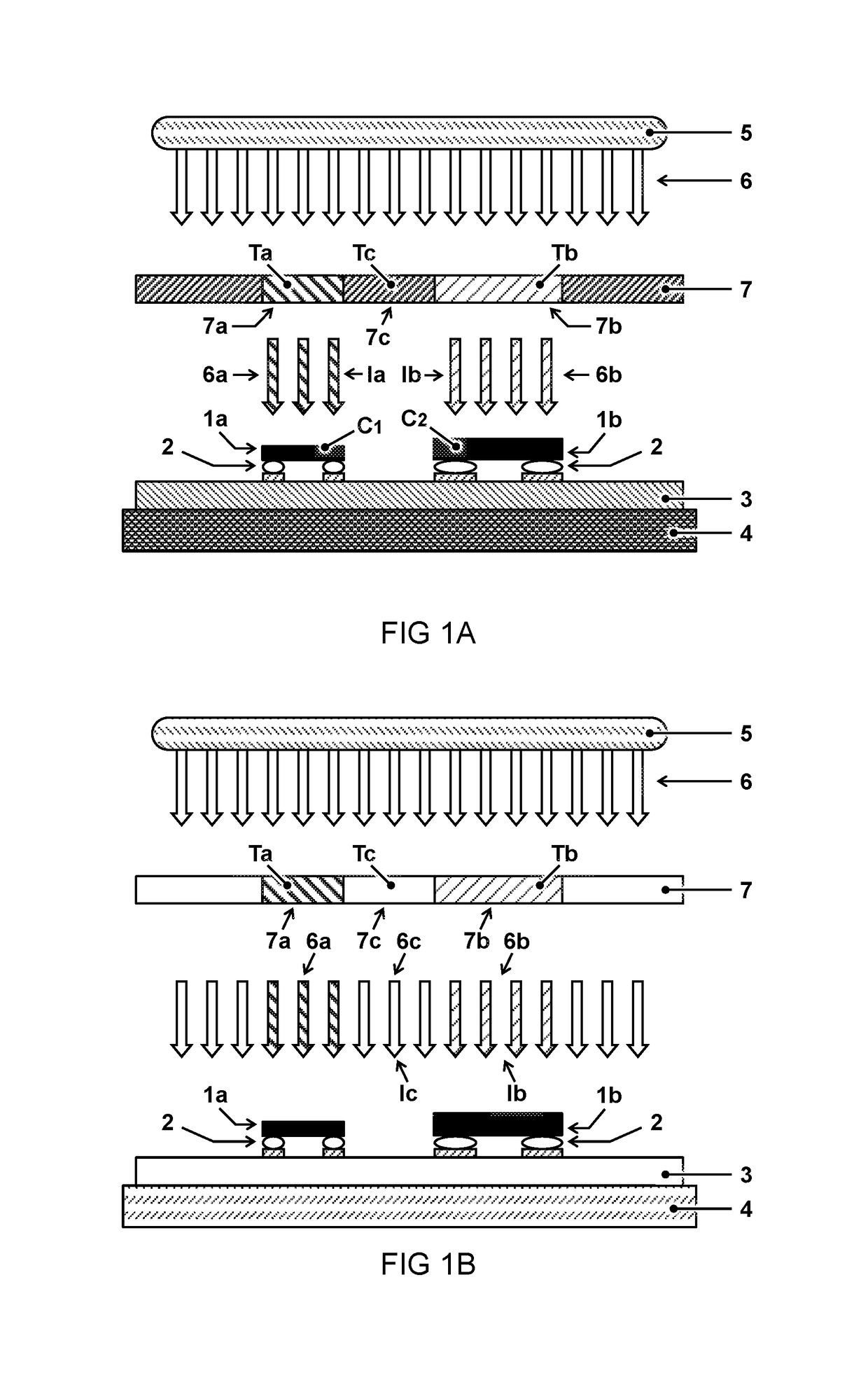
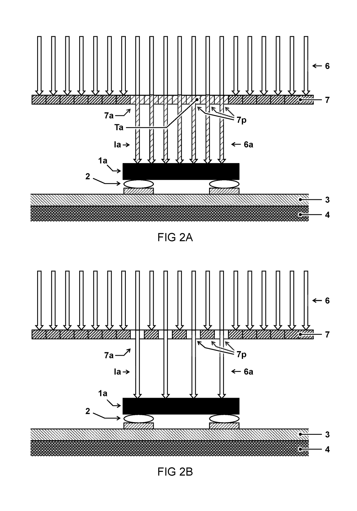
[0008]The inventors note that different heating properties of chips may cause the chips to heat differently, e.g. to reach different temperatures, when their respective illuminated areas are exposed to the same (homogeneous) light intensity, in particular by being exposed to a single flash light pulse. Using different light intensities, e.g. power or energy per unit area, may at least partially compensate the different heating properties of the chips to reduce a spread in temperature between the chips as a result of the heating by the light pulse. The different chips may e.g. attain a predetermined temperature in a small temperature range for melting the solder material in contact therewith in a controlled manner. It will be appreciated that the present technique has the advantages of a flash lamp exposure, e.g. being relatively fast being able to expose large areas with multiple components, compatible with flexible foils and roll-to-roll processing due to the pulse duration and intensity. Furthermore, by use of the masking device, the technique can be reliable, e.g. due to improved control over the heating of different chips. The masking device can also be used to prevent exposure of the substrate, e.g. at places between the chips. This may prevent damage to the substrate.
[0010]The masking device can be based on reflection and / or transmission and may comprise e.g. a fixed or variable mask pattern. For example, a variable mask pattern can be achieved by electronic control of (an array of) digital mirrors or other tuneable optics. A variable mask pattern may be formed e.g. by a grid of pixels that can switch their transmission coefficient depending on a control signal. A variable light intensity can e.g. be achieved by setting multiple pixels to the same specific transmission coefficient or by using a combination of pixels with different transmission coefficients combined. Advantageously, a pixelated mask can be used to selectively heat only part of the chip. This can leverage the process by avoiding damaging sensitive part of the chip or enhancing heat flow from (part of) the chip, e.g. close to the solder bumps. For example, a dithered pattern can be formed wherein some pixels completely block the light from reaching the chip (i.e. transmission coefficient zero), while neighbouring pixels pass the light. Also other combinations of patterns and different (non-zero) transmission coefficients are possible.
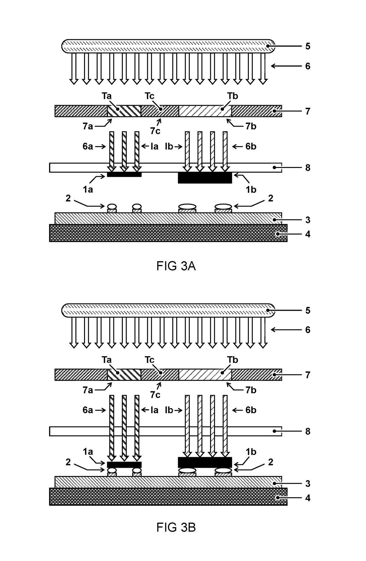
[0012]By projecting the light pulse onto the chips while they are positioned on the substrate with the solder material there between, the chips can be heated and cause at least partial melting of the solder material for attaching the chips to the substrate. Alternatively, or in addition, chips can also be first provided on a chip carrier substrate before being transferred to the destination substrate. Advantageously, the light pulse can be used for both releasing the chips from the carrier substrate and heating the chips for soldering. For example, chips can be released from the substrate by decomposition or ablation of material of the chip carrier by the heated chip. The chips may also be continuously heated while in mid air between the carrier and destination substrate. The chip can be heated relatively fast while in mid air if it is not contacting a heat sink, such as the substrate, and a relatively high temperature can be achieved. By modulating an intensity of the pulse, it can be adapted to different phases of the transfer, e.g. with less intensity during the transfer in mid air to prevent overheating. Light modulation can e.g. be effected by the masking device and / or control of the flash lamp.
[0013]The transfer of chips from a carrier can also be performed without a masking device. Accordingly, another or further aspect of the present disclosure provides a method for soldering a chip to a substrate comprising providing a substrate and a flash lamp with a chip carrier there between. According to the method, one or more chips are attached to the chip carrier on a side of the chip carrier facing the substrate. A flash lamp is provided generating a light pulse for heating the chip. The heating of the chip causes the chip to be released from the chip carrier towards the substrate. Advantageously, the method can provide contactless transfer of one or more chips to a substrate.
[0018]For example, chips can be positioned on the substrate by a chip supply unit, such as a pick and place device, with the solder material there between before being illuminated by a light pulse. Alternatively, chips can be placed by illumination a chip carrier foil that releases the chips over the substrate while simultaneously heating the chip for soldering. By additionally using the masking device, chips with different heating properties, e.g. different sizes, can be contactlessly transferred from the carrier to the destination substrate. The masking device and the chip carrier can be separate devices or integrated as a single piece, e.g. comprised in a flexible foil. The chip carrier and / or masking device can be moved in synchronicity with the substrate to place the chips at the intended locations while keeping the substrate moving e.g. in a roll-to-roll process. Alternatively, or in addition, the substrate handler may slow down or stop movement of the substrate while the light is applied to the chips.

Problems solved by technology

However, for more complex systems, there is a need to develop hybrid systems in which printed circuitry is combined with silicon-based integrated circuits or surface mounted device (SMD) components, referred herein as chip components or simply “chips”.
However, these processes are considered time consuming and / or incompatible with low-cost foils having low decomposition temperatures.
However, reflow soldering, is poorly compatible with low-cost flexible foils and roll-to-roll (R2R) processing because it requires maintaining the whole board above the liquidus temperature of the solder for long holding time.
This can result in a time-consuming process using large in-line ovens, often having multiple loops.
The long holding time may also cause deformation or degradation of the flexible foil itself or degradation of its organic surface coatings or adhesives.
However, in laser spot soldering, the small spot area may require precise positioning of the spot for each component.
Furthermore, applying this technology in a R2R process is challenging as the laser spot needs to align to multiple chips on a moving substrate.
Furthermore, the process can be time consuming.
However, if the absorption of light by the (foil) substrate and / or components differs, this can lead to selective heating.
This may lead to further differences in heating behaviour for the different components, which makes the temperature and solder process difficult to control.

Method used


Image

  • Apparatus and method for soldering a plurality of chips using a flash lamp and a mask
  • Apparatus and method for soldering a plurality of chips using a flash lamp and a mask
  • Apparatus and method for soldering a plurality of chips using a flash lamp and a mask

Examples


Embodiment Construction

[0028]In some instances, detailed descriptions of well-known devices and methods may be omitted so as not to obscure the description of the present systems and methods. Terminology used for describing particular embodiments is not intended to be limiting of the invention. As used herein, the singular forms “a”, “an” and “the” are intended to include the plural forms as well, unless the context clearly indicates otherwise. The term “and / or” includes any and all combinations of one or more of the associated listed items. It will be understood that the terms “comprises” and / or “comprising” specify the presence of stated features but do not preclude the presence or addition of one or more other features. It will be further understood that when a particular step of a method is referred to as subsequent to another step, it can directly follow said other step or one or more intermediate steps may be carried out before carrying out the particular step, unless specified otherwise. Likewise i...


PUM

PropertyMeasurementUnit
liquidus temperatureaaaaaaaaaa
thickaaaaaaaaaa

Abstract

A substrate (3) and two or more different chips (1a, 1b) having different heating properties (e.g. caused by different dimensions (surface area and / or thickness), heat capacity (C1, C2), absorptivity, conductivity, number and / or size of solder bonds) are provided. A solder material (2) is disposed between the chips (1a, 1b) and the substrate (3). A flash lamp (5) generates a light pulse (6) for heating the chips (1a, 1b), wherein the solder material (2) is at least partially melted by contact with the heated chips (1a, 1b). A masking device (7) is disposed between the flash lamp (5) and the chips (1a, 1b) causing different light intensities (1a, 1b) in different areas (6a, 6b) of the light pulse (6) passing the masking device (7), thereby heating the chips (1a, 1b) with different light intensities (1a, 1b). This may compensate the different heating properties to reduce a spread in temperature between the chips (1a, 1b) as a result of the heating by the light pulse (6). The chips (1a, 1b) may be releasably carried by a chip carrier disposed between the flash lamp (5) and the substrate (3) before being positioned on the substrate (3), wherein the light (6a, 6b) of the light pulse (6) transmitted by the masking device (7) is projected onto the chips (1a, 1b) held by the chip carrier for heating the chips (1a, 1b), releasing them from the chip carrier and transferring them to the substrate (3), wherein the heated chips (1a, 1b) cause melting of the solder material (2) between the chips (1a, 1b) and the substrate (3) for attaching the chips (1a, 1b) to the substrate (3).

Description

TECHNICAL FIELD AND BACKGROUND[0001]The present disclosure relates to soldering, in particular to an apparatus and method for soldering chips to a substrate.[0002]Simple flexible systems, such as logic functions with transistors or optoelectronic devices, can in principle be fully printed on a substrate (e.g. foil or rigid board). However, for more complex systems, there is a need to develop hybrid systems in which printed circuitry is combined with silicon-based integrated circuits or surface mounted device (SMD) components, referred herein as chip components or simply “chips”. To functionalize the device, multiple chip components, often having different dimensions, may need to be interconnected to the circuit tracks on the substrate, e.g. printed or etched copper circuits. This can be realized for example using oven reflow soldering, conducting adhesive bonding or face-up chip integration. However, these processes are considered time consuming and / or incompatible with low-cost foi...

Claims


Application Information

Patent Timeline
Patent Type & Authority Applications(United States)
IPC IPC(8): H01L23/00H01L21/683H05K3/34
CPCH01L24/75H01L21/6836H01L24/11H01L24/97H01L24/81H05K3/3436H05K3/3494H01L24/16H01L24/13H01L2224/8119H01L2224/81815H01L2224/8123H01L2224/81224H01L2224/97H01L2221/68354H01L2224/131H01L21/6835H05K2201/0145H01L2224/1132H01L2224/1131H01L2221/68381H01L2224/16227H01L2224/7565H01L2224/75611H01L2224/75502H01L2224/75253H01L2224/7526H01L2224/75252H01L2224/7598H01L2224/759H01L2224/75824H01L2224/75804H01L2224/75753H01L2224/75702H01L2224/81193H01L2224/81191H01L2224/81192H01L2224/81005H01L2924/014H01L2224/81H01L2924/00012H01L2924/00014Y02P70/50
Inventor ARUTINOV, GARISMITS, EDSGER CONSTANT PIETERVAN DEN BRAND, JEROEN
Owner NEDERLANDSE ORG VOOR TOEGEPAST-NATUURWETENSCHAPPELIJK ONDERZOEK (TNO)
Why Eureka
Try Eureka