Charged Particle Beam Device
- Summary
- Abstract
- Description
- Claims
- Application Information
AI Technical Summary
Benefits of technology
Problems solved by technology
Method used
Image

Examples
Embodiment Construction
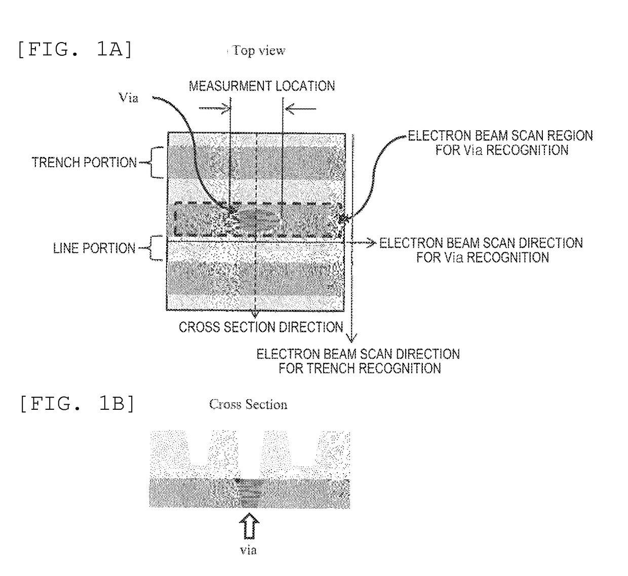
[0033]In recent years, as the miniaturization of semiconductor devices, the aspect ratio (depth / width) of trenches (groove-shaped patterns) or vias (hole patterns) tends to increase. As a result, it is difficult to detect the signal of the via edge or the trench bottom. In addition, it is necessary to use double patterning such as SADP (Self Aligned Double Patterning) in formation of fine vias or trenches, thereby being affected by various processes such as film formation or etching. Therefore, it is necessary to manage not only the dimension of vias or trenches but also the positional deviation, the residual film or the like.
[0034]In the embodiment described below, an electron beam scan is performed in a direction conforming to patterns, so that a measurement target pattern is pinpointedly captured to facilitate improvement of throughput by shortening the capturing time. Particularly, it is effective for the measurement of a multilayer structure such as a via in trench illustrated ...
PUM
 Abstract
Description
Claims
Application Information
 - R&D Engineer
- R&D Manager
- IP Professional
- Industry Leading Data Capabilities
- Powerful AI technology
- Patent DNA Extraction
Browse by: Latest US Patents, China's latest patents, Technical Efficacy Thesaurus, Application Domain, Technology Topic.
© 2024 PatSnap. All rights reserved.Legal|Privacy policy|Modern Slavery Act Transparency Statement|Sitemap