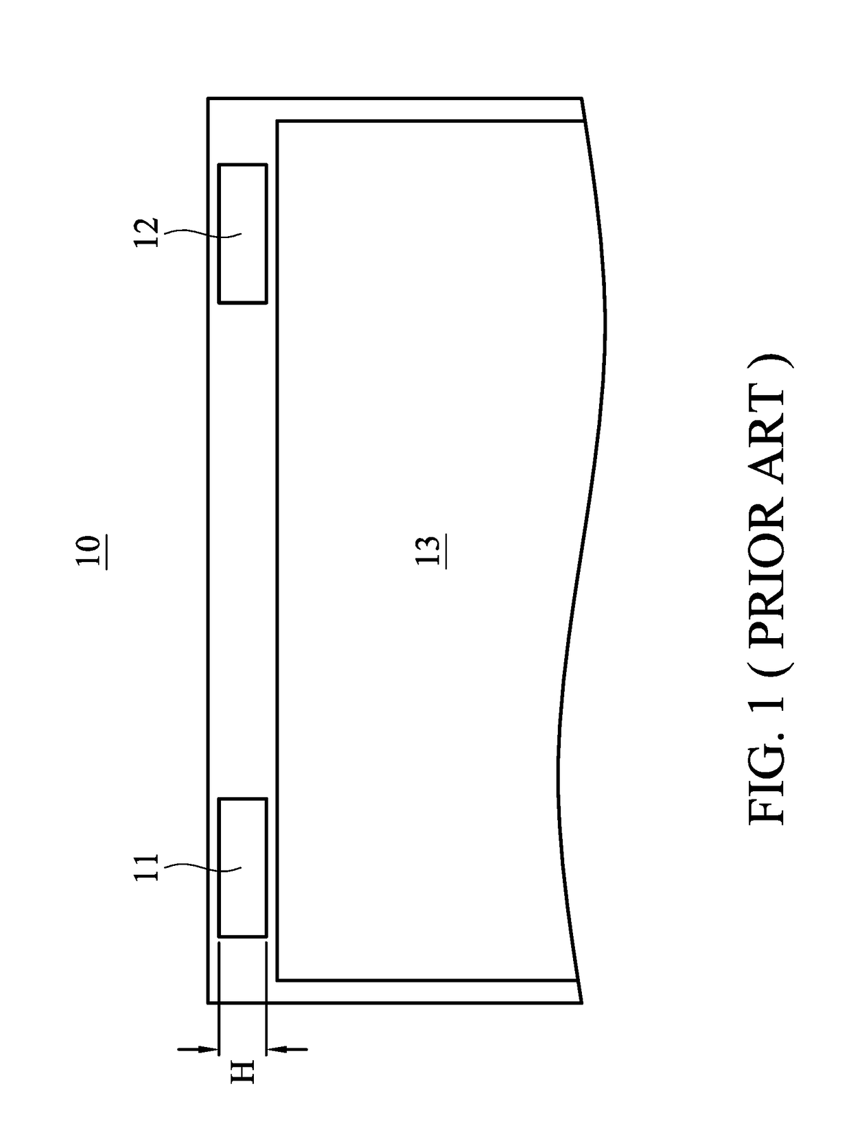
Dual-band antenna structure
- Summary
- Abstract
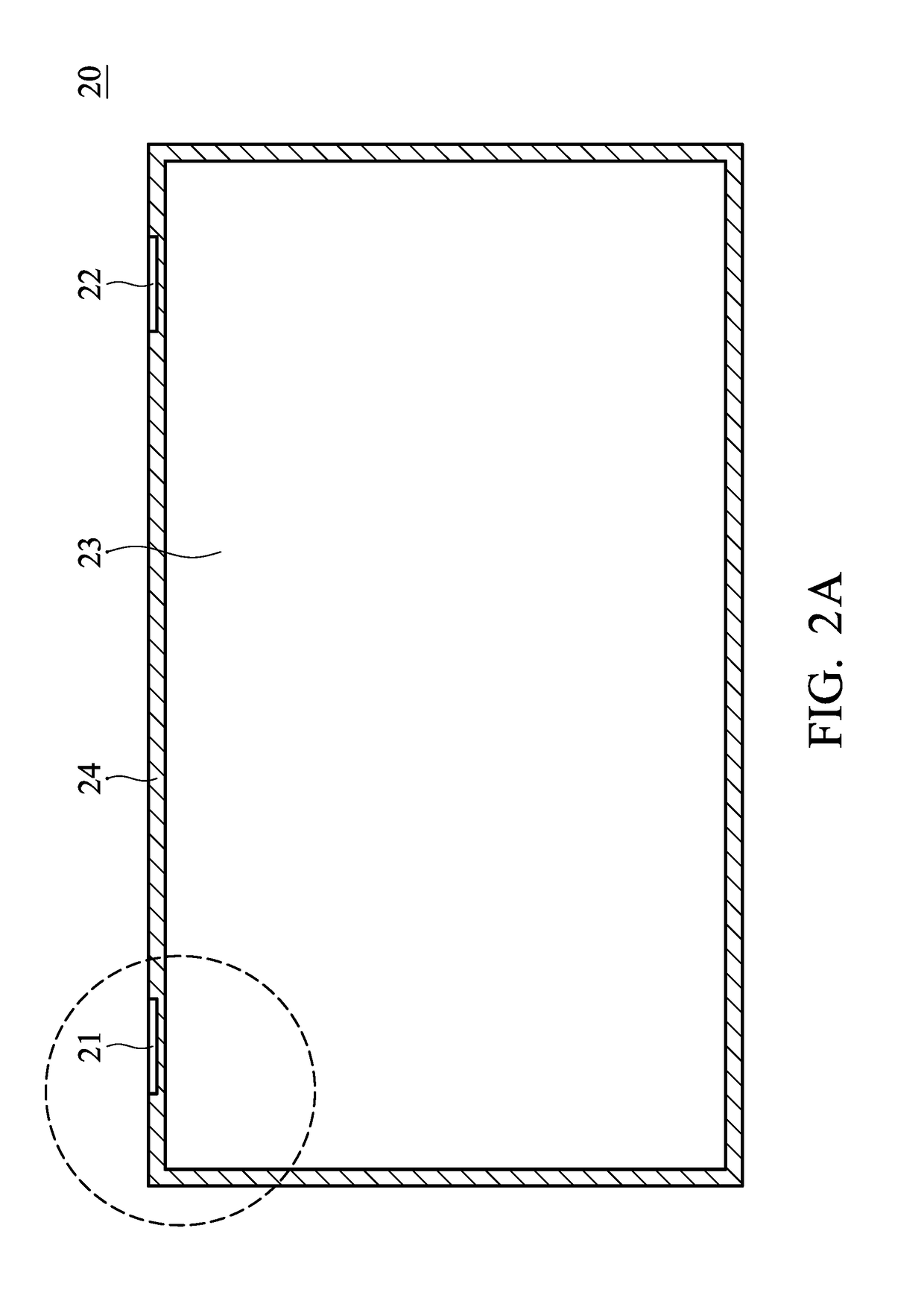
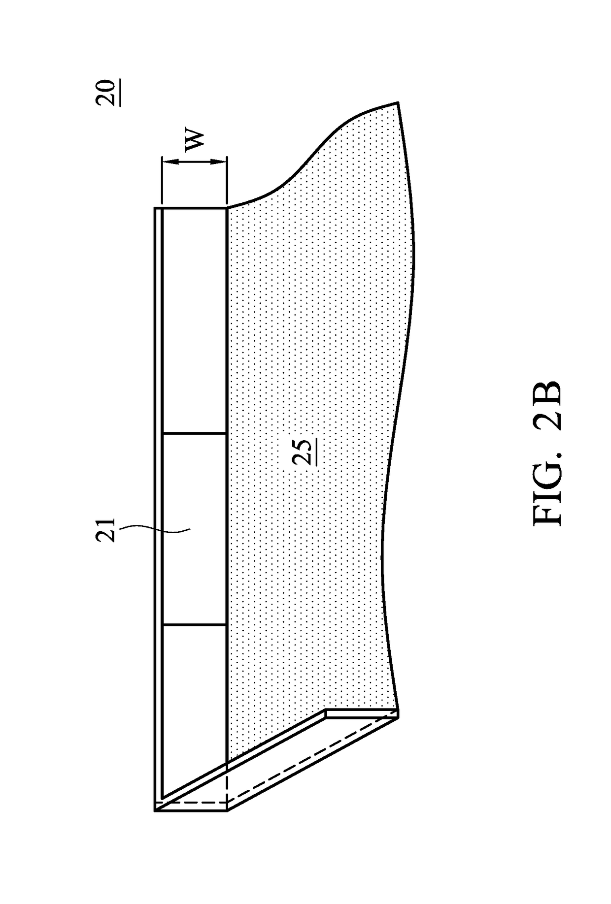
- Description
- Claims
- Application Information
AI Technical Summary
Benefits of technology
Problems solved by technology
Method used
Image

Examples
first embodiment
[0028]In the first embodiment, the signal source 31 is considered as an input terminal or an output terminal of the antenna structure 3. The first feeding arm 33 is electrically coupled to the signal source 31. The second feeding arm 34 is electrically coupled to the signal source 31. The first radiation arm 35 has a first open end 351 and a first grounding point 352. The first radiation arm 35 is electrically coupled to a bending element 353. The first grounding point 352 is electrically coupled to the system ground plane 30. The second radiation arm 36 has a second open end 361 and a second grounding point 362. The first open end 351 and the second open end 361 are opposite to each other. The second grounding point 362 is electrically coupled to the system ground plane 30. The first feeding arm 33 is disposed between the first radiation arm 35 and the system ground plane 30. The second feeding arm 34 is disposed between the second radiation arm 36 and the system ground plane 30. A...
second embodiment
[0035]In the second embodiment, the signal source 61 is considered as an input terminal or an output terminal of the antenna structure 6. The first feeding arm 63 is electrically coupled to the signal source 61. The second feeding arm 64 is electrically coupled to the signal source 61. The first radiation arm 65 has a first open end 651 and a first grounding point 652. The first radiation arm 65 is electrically coupled to an inductive element 653. The inductive element 653 may be a chip inductive element or a distributed inductive element. The first grounding point 652 is electrically coupled to the system ground plane 60. The second radiation arm 66 has a second open end 661 and a second grounding point 662. The first open end 651 and the second open end 661 are opposite to each other. The second grounding point 662 is electrically coupled to the system ground plane 60. The first feeding arm 63 is disposed between the first radiation arm 65 and the system ground plane 60. The secon...
third embodiment
[0041]In the third embodiment, the signal source 71 is considered as an input terminal or an output terminal of the antenna structure 7. The first feeding arm 73 is electrically coupled to the signal source 71. The second feeding arm 74 is electrically coupled to the signal source 71. The first radiation arm 75 has a first open end 751 and a first grounding point 752. The first radiation arm 75 is electrically coupled to a bending element 753. The first grounding point 752 is electrically coupled to the system ground plane 70. The second radiation arm 76 has a second open end 761 and a second grounding point 762. The first open end 751 and the second open end 761 are opposite to each other. The second grounding point 762 is electrically coupled to the system ground plane 70.
[0042]In the third embodiment, the first feeding arm 73 and the second feeding arm 74 are disposed on the first radiation arm 75 and the second radiation arm 76. More specifically, the first radiation arm 75 is d...
PUM
 Abstract
Description
Claims
Application Information
 - Generate Ideas
- Intellectual Property
- Life Sciences
- Materials
- Tech Scout
- Unparalleled Data Quality
- Higher Quality Content
- 60% Fewer Hallucinations
Browse by: Latest US Patents, China's latest patents, Technical Efficacy Thesaurus, Application Domain, Technology Topic, Popular Technical Reports.
© 2025 PatSnap. All rights reserved.Legal|Privacy policy|Modern Slavery Act Transparency Statement|Sitemap|About US| Contact US: help@patsnap.com