Goa circuit and liquid crystal display device

Active Publication Date: 2019-02-14
SHENZHEN CHINA STAR OPTOELECTRONICS SEMICON DISPLAY TECH CO LTD
View PDF2 Cites 5 Cited by
  • Summary
  • Abstract
  • Description
  • Claims
  • Application Information

AI Technical Summary

Benefits of technology

[0035]In summary, the GOA circuit and the liquid crystal display device of the present invention can enhance the performance of t

Problems solved by technology

However, in the case where the start signal STV is currently used as the GOA ON signal and the Q-point pre-charging signal, the waveforms o

Method used


Image

  • Goa circuit and liquid crystal display device
  • Goa circuit and liquid crystal display device
  • Goa circuit and liquid crystal display device

Examples


Embodiment Construction

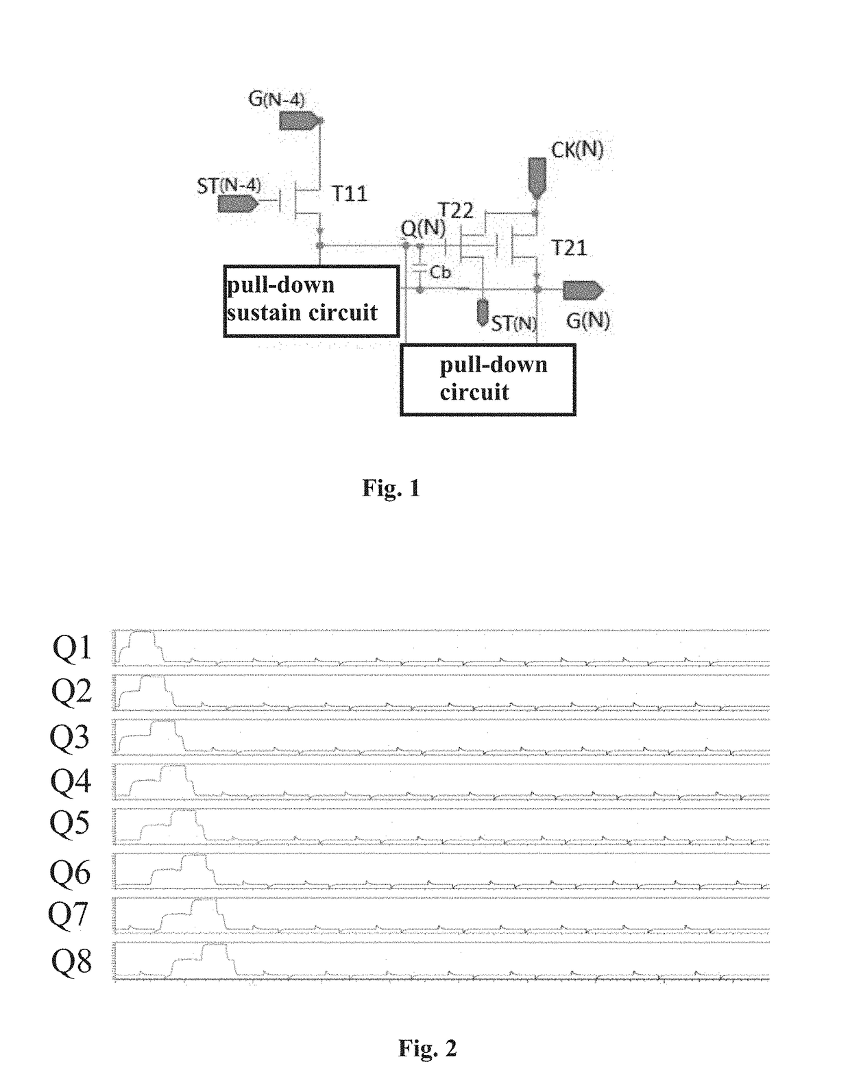
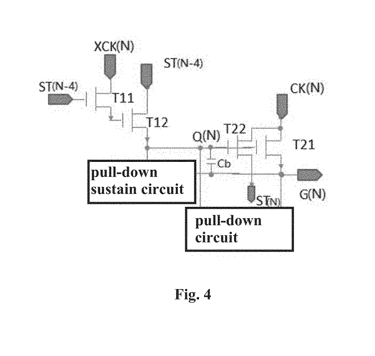
[0044]Please refer to FIG. 4, which is an illustrative diagram of a GOA circuit structure of a preferred embodiment according to the present invention. The GOA circuit structure is mainly constituted by the pull-high control circuit T11, the pull-high circuit (including T21, T22), the pull-down circuit, the pull-down sustain circuit, and a boast capacitor Cb and so on.

[0045]To the N-th stage GOA unit, the pull-high control circuit is responsible for controlling the opening time of the pull-high circuit and pre-charging the node Q (N). The pull-up circuit is connected with a high-frequency clock signal CK (N) and stage-transfer signal output terminal of the N-th stage GOA unit (N) for outputting the clock signal CK (N) to the corresponding horizontal scanning line through the gate signal output terminal G (N) of the N-th stage and outputting the stage-transfer signal of the N-th stage GOA unit. The pull-down circuit is responsible for pulling down the potential of the gate signal out...


PUM


Abstract

The present invention involves a GOA circuit and a liquid crystal display. The GOA circuit comprises an N-th stage GOA unit, which comprises a pull-high control circuit, a pull-high circuit, a pull-down circuit, a pull-down sustain circuit, and a boast capacitor (Cb). A first clock signal CK(N) is inputted to the pull-high circuit. The pull-high control circuit comprises: A first thin film transistor (T11), whose gate electrode is connected with a stage-transfer signal output terminal of the (N-m)th stage GOA unit, whose source electrode and drain electrode are respectively connected with a gate electrode of a second thin film transistor (T12) and inputted with a second clock signal (XCK(N)). A source electrode and a drain electrode of the second thin film transistor (T12) are respectively connected with the stage-transfer signal output terminal of the (N-m)th stage GOA unit and the node (Q(N)) of the N-th stage GOA unit. The present invention also provides a corresponding liquid crystal display device. The GOA circuit and the liquid crystal display device of the present invention can make the output waveform of the node Q of each GOA unit be consistent.

Description

BACKGROUND OF THE INVENTION[0001]Field of Invention[0002]The present invention relates to the field of liquid crystal display, and more particularly to a GOA circuit and a liquid crystal display device.[0003]Description of Prior Art[0004]Liquid crystal displays (LCDs) such as flat panel display devices are widely used in mobile phones, televisions, personal digital assistants, digital cameras, notebooks, desktop, other consumer electronics products and etc. for high quality, power saving, thin body and wide application range. The LCDs has become the mainstream in display device.[0005]In the active LCD, each sub-pixel has a thin film transistor (TFT) whose gate electrode is connected with a horizontal scanning line, a drain electrode is connected with a data line in the vertical direction, and a source electrode is connected with a pixel electrode. Applying a sufficient voltage on the horizontal scanning line, all the TFTs on the horizontal scanning line are opened, where the pixel e...

Claims


Application Information

Patent Timeline
IPC IPC(8): G09G3/36
CPCG09G3/3677G09G2310/06G09G2310/08G09G3/3674G09G2310/0286G11C19/28
Inventor WANG, TIANHONGCHEN, SHUJHIH
Owner SHENZHEN CHINA STAR OPTOELECTRONICS SEMICON DISPLAY TECH CO LTD
Why Eureka
Try Eureka