
Inverted quantum dot light-emitting diode and manufacturing method thereof

a light-emitting diode and quantum dot technology, applied in the field of display technology, can solve the problems of reducing the life span of the device, limiting the luminous efficiency of the device, and lowering the electron transport rate, so as to overcome the deficiencies of inhomogeneous film formation, low light extraction efficiency, and low efficiency

Active Publication Date: 2019-02-28
SHENZHEN CHINA STAR OPTOELECTRONICS SEMICON DISPLAY TECH CO LTD
View PDF4 Cites 7 Cited by
  • Summary
  • Abstract
  • Description
  • Claims
  • Application Information

AI Technical Summary

Benefits of technology

The present invention provides an inverted quantum dot light-emitting diode (QD-LED) and a manufacturing method that overcomes issues of inhomogeneous film formation and low light extraction efficiency. The method uses a hydrothermal synthesis process to form a monocrystalline TiO2 nanorod array film that serves as an electron transport layer. This ensures high-efficiency electron transport, increased scattering of light, and improved luminous efficiency and stability of the device. The resulting QD-LED also demonstrates increased luminous efficiency and stability.

Problems solved by technology

Although ZnO or TiO2 provide excellent electron transport speeds, yet the nanometer particles show poor property of dispersion and are unstable, making them easy to aggregate and thus leading to lowering of electron transport rate and directly resulting in inhomogeneity of a film surface, thereby limiting the luminous efficiency of a device and reducing the life span of the device.

Method used


Image

  • Inverted quantum dot light-emitting diode and manufacturing method thereof
  • Inverted quantum dot light-emitting diode and manufacturing method thereof
  • Inverted quantum dot light-emitting diode and manufacturing method thereof

Examples


Embodiment Construction

[0051]To further expound the technical solution adopted in the present invention and the advantages thereof, a detailed description will be given with reference to the preferred embodiments of the present invention and the drawings thereof.

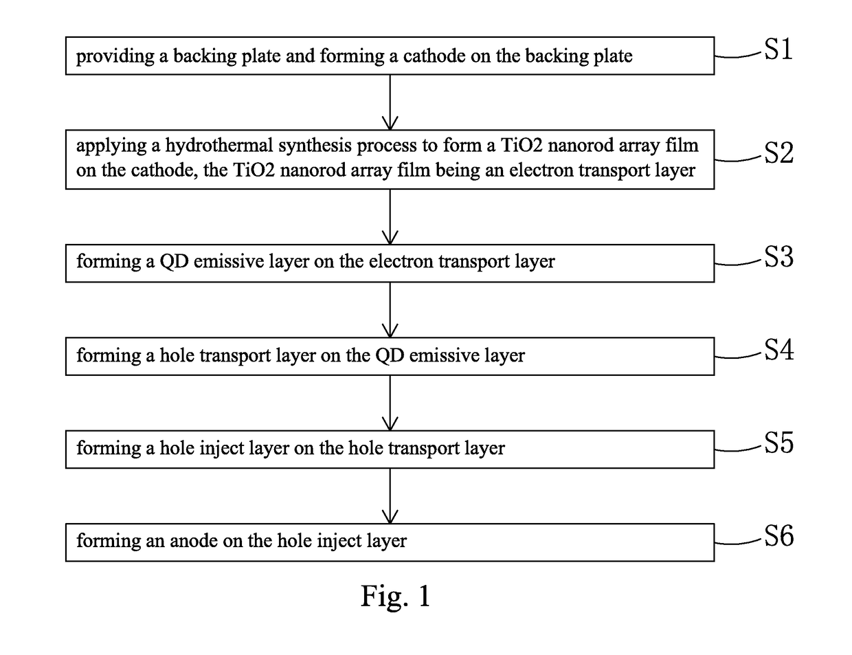
[0052]Referring to FIG. 1, the present invention provides a manufacturing method of an inverted quantum dot light-emitting diode (QD-LED), which comprises the following steps:

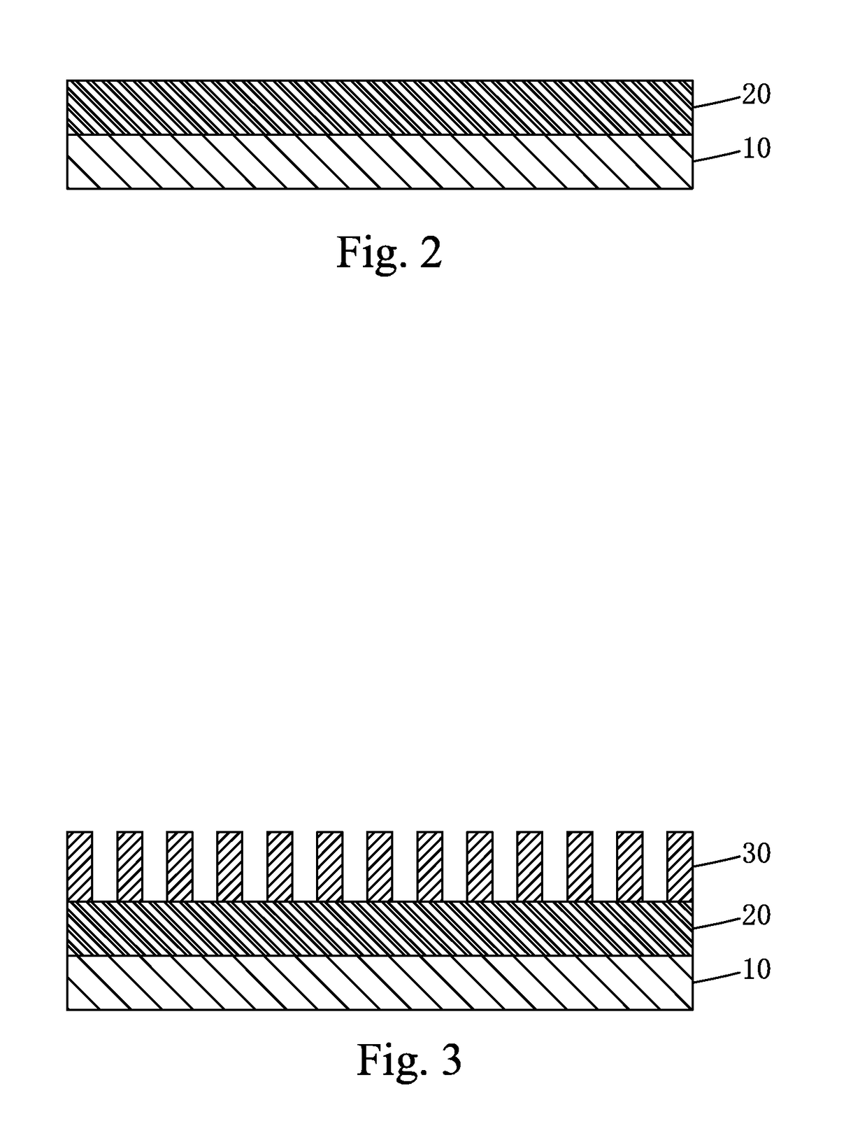
[0053]Step S1: as shown in FIG. 2, providing a backing plate 10 and forming a cathode 20 on the backing plate 10

[0054]Specifically, the backing plate 10 comprises a flexible backing.

[0055]Specifically, a magnetron sputtering film forming process is adopted to form the cathode 20. The cathode 20 is formed of a material that comprises a transparent conductive metal oxide. The cathode 20 has a film thickness that is between 20 nm and 200 nm. Preferably, the transparent conductive metal oxide comprises indium tin oxide (ITO).

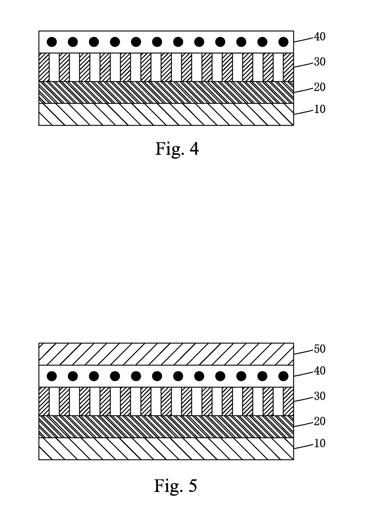
[0056]Step S2: as shown in FIG. 3, applying a hydrother...


PUM

PropertyMeasurementUnit
thicknessaaaaaaaaaa
thicknessaaaaaaaaaa
thicknessaaaaaaaaaa

Abstract

The present invention provides an inverted QD-LED and a manufacturing method thereof. The manufacturing method of an inverted QD-LED according to the present invention adopts a hydrothermal synthesis process to form a monocrystalline TiO2 nanorod array film for serving as an electron transport layer, wherein a plurality of monocrystalline TiO2 nanorods contained in the monocrystalline TiO2 nanorod array film are arranged in an array so as not to readily get aggregated thereby overcoming the deficiencies of inhomogeneous film formation resulting from aggregation of TiO2 nanometer particles, lowered electron transport efficiency, and low light extraction efficiency, and thus ensuring high-efficiency electron transport rate of the electron transport layer, increasing scattering of light to heighten light extraction efficiency, and improve luminous efficiency and stability of a device. The inverted QD-LED according to the present invention involves a monocrystalline TiO2 nanorod array film to serve as an electron transport layer, and thus demonstrates increased luminous efficiency and stability.

Description

BACKGROUND OF THE INVENTION1. Field of the Invention[0001]The present invention relates to the field of display technology, and more particular to an inverted quantum dot light-emitting diode (QD-LED) and a manufacturing method thereof.2. The Related Arts[0002]With the continuous development of the display technology, people increasingly demand higher and higher quality of displaying. Quantum dots (QDs) are nanometer semiconductor particles in the form of spheres or similar to spheres made of elements of II-VI groups or III-V groups, having a particle size between several nanometers and tens of nanometers. Since the particle size of QDs is less than or close to the exciton Bohr radius of the corresponding body material, an quantum confinement effect is generally involved, where the energy band structure is changed from quasi-continuity of the body material to the discrete structure of the quantum dot material, making the quantum dots exhibiting unique behavior of stimulated emission...

Claims


Application Information

Patent Timeline
Patent Type & Authority Applications(United States)
IPC IPC(8): H01L51/50H01L51/52H01L51/56H10K99/00
CPCH01L51/5072H01L51/502H01L51/5234H01L51/56H01L51/5088H01L51/5056H01L2251/5353H01L2251/308H01L2251/5369H01L51/0037H01L51/0035H01L51/0042H01L2251/558H01L2251/301H10K50/115H10K50/16H10K2102/321H10K2102/331H10K50/17H10K50/828H10K71/00H10K71/12H10K50/15H10K85/111H10K85/146H10K85/1135H10K2102/00H10K2102/103H10K2102/351
Inventor XIAO, YADAN
Owner SHENZHEN CHINA STAR OPTOELECTRONICS SEMICON DISPLAY TECH CO LTD
Learn More