Micro-Nano Textured Graphene-Based Bionic PH Sensor and Preparation Method Therefor
a bionic ph sensor and nano-textured technology, applied in nanomedicine, material electrochemical variables, instruments, etc., can solve the problems of inability to solve ph in-situ measurement of heterogeneous environments such as soils and cultivation substrates, and achieve the effects of improving the performance of ph sensors, reducing reaction time, and rapid measuremen
- Summary
- Abstract
- Description
- Claims
- Application Information
AI Technical Summary
Benefits of technology
Problems solved by technology
Method used
Image

Examples
embodiment 1
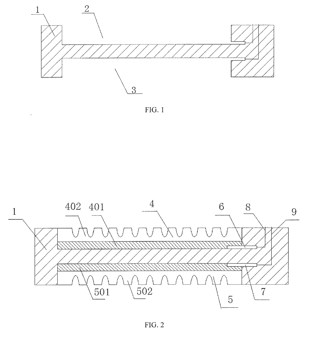
[0027]S1. Slotting on the two sides of the substrate 1 to prepare slot A 2 and slot B 3. Then setting the copper contact A 6 and copper contact B 7 on the bottom of slot A 2 and slot B 3, and connected with the inner lead A 8 and inner lead B 9 respectively.
[0028]S2. Through the method of micro mechanical peeling transfer, graphene A 401 is deposited on the upper surface of copper contact A 6 and slot A 2 by graphene film whose thickness is 5 nm, while graphene B 501 is deposited on the upper surface of copper contact B 7 and slot B 3. Antimony is used to prepare the sensitive electrode material layer 402 on the upper surface of graphene A 401 by magnetron sputtering method, the vacuum is 3×10⁻⁴ Pa, the process pressure is 1 Pa, the power is 50 W, the shielding gas is argon, the flow is 39 sccm, and the time is 40 min. Using femtosecond laser processing equipment to process micro-pits on the surface of the sensitive electrode material layer 402, the hole depth is ˜80 nm, the hole di...
embodiment 2
[0030]S1. Slotting on the two sides of the substrate 1 to prepare groove A 2 and slot B 3. Then setting the copper contact A 6 and copper contact B 7 on the bottom of slot A 2 and slot B 3, and connected with the inner lead A 8 and inner lead B 9 respectively.
[0031]S2. Through the method of micro mechanical peeling transfer, graphene A 401 is deposited on the upper surface of copper contact A 6 and slot A 2 by graphene film whose thickness is 10 nm, while graphene B 501 is deposited on the upper surface of copper contact B 7 and slot B 3. Ruthenium oxide is used to prepare the sensitive electrode material layer 402 on the upper surface of graphene A 401 by magnetron sputtering method. The sputtering is completed at room temperature, the vacuum is 3×10⁻⁴ Pa, the process pressure is 1 Pa, the power is 100 W, the concentration ratio of argon and oxygen is 9:1, the flow is 45 sccm, and the time is 90 min. The micro-pits whose depth is ˜80 nm and diameter is ˜2 μm is processed on the sur...
PUM
 Abstract
Description
Claims
Application Information
 - R&D Engineer
- R&D Manager
- IP Professional
- Industry Leading Data Capabilities
- Powerful AI technology
- Patent DNA Extraction
Browse by: Latest US Patents, China's latest patents, Technical Efficacy Thesaurus, Application Domain, Technology Topic.
© 2024 PatSnap. All rights reserved.Legal|Privacy policy|Modern Slavery Act Transparency Statement|Sitemap