

Planarization Process and Apparatus
a technology of planarization and apparatus, applied in the direction of photomechanical treatment, semiconductor/solid-state device testing/measurement, instruments, etc., can solve the problems of difficult and expensive to implement and maintain, difficult and expensive to apply cmp to soft materials, and negative impact of variation on the ability to add additional layers to layered substrates
- Summary
- Abstract
- Description
- Claims
- Application Information
AI Technical Summary
Benefits of technology
Problems solved by technology
Method used
Image

Examples
Embodiment Construction
[0042]What is needed are systems and processes which will meet aggressive planarization targets. One method of meeting these aggressive planarization targets is to use a planarization method that includes depositing a planarizing formable material onto a wafer surface and cure the formable material using a whole wafer imprint tool. The applicant has determined that varying the drop pattern and deforming the template are not sufficient to compensate for the dual parasitic effect of both volume shrinkage and pattern density variation due to boundary condition effects at low pattern density regions. For aggressive planarization targets these compensation techniques are insufficient. The aggressive planarization targets may be within just individual die, within an imprint field or exposure field, or across the substrate.
Planarization System
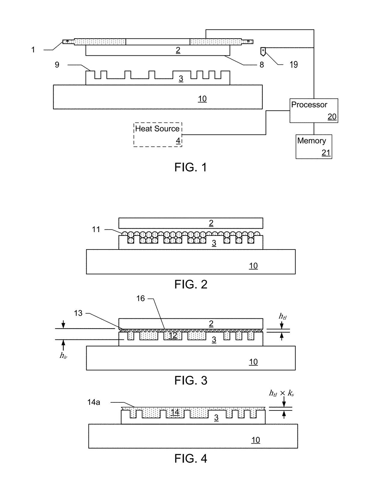
[0043]FIG. 1 is schematic of an imprint type planarization tool. A superstrate chuck 1 may support a superstrate and is configured to position the su...
PUM
| Property | Measurement | Unit |
|---|---|---|
| thickness | aaaaa | aaaaa |
| thickness | aaaaa | aaaaa |
| thickness | aaaaa | aaaaa |
Abstract
Description
Claims
Application Information