Nano multi-step height sample plate and its preparation
A high-profile, step-height technology, applied in the field of micro-nano testing, can solve problems such as harsh processing conditions and high costs, and achieve the effects of low cost, diverse material choices, and good manufacturability
- Summary
- Abstract
- Description
- Claims
- Application Information
AI Technical Summary
Problems solved by technology
Method used
Image
Examples
Embodiment Construction
[0023] The present invention will be described in further detail below in conjunction with the accompanying drawings.
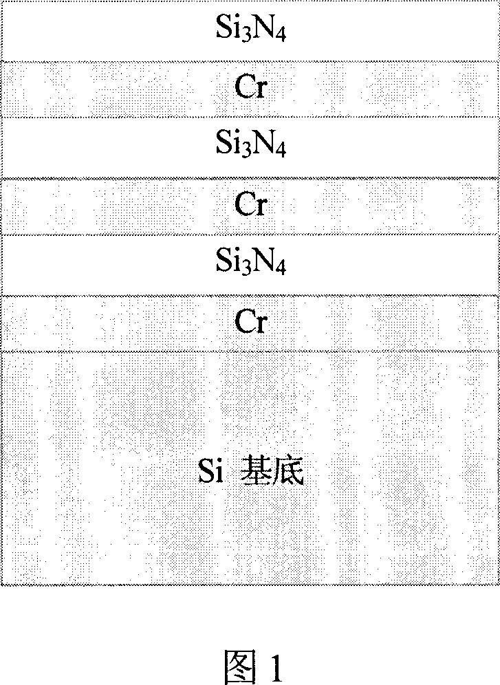
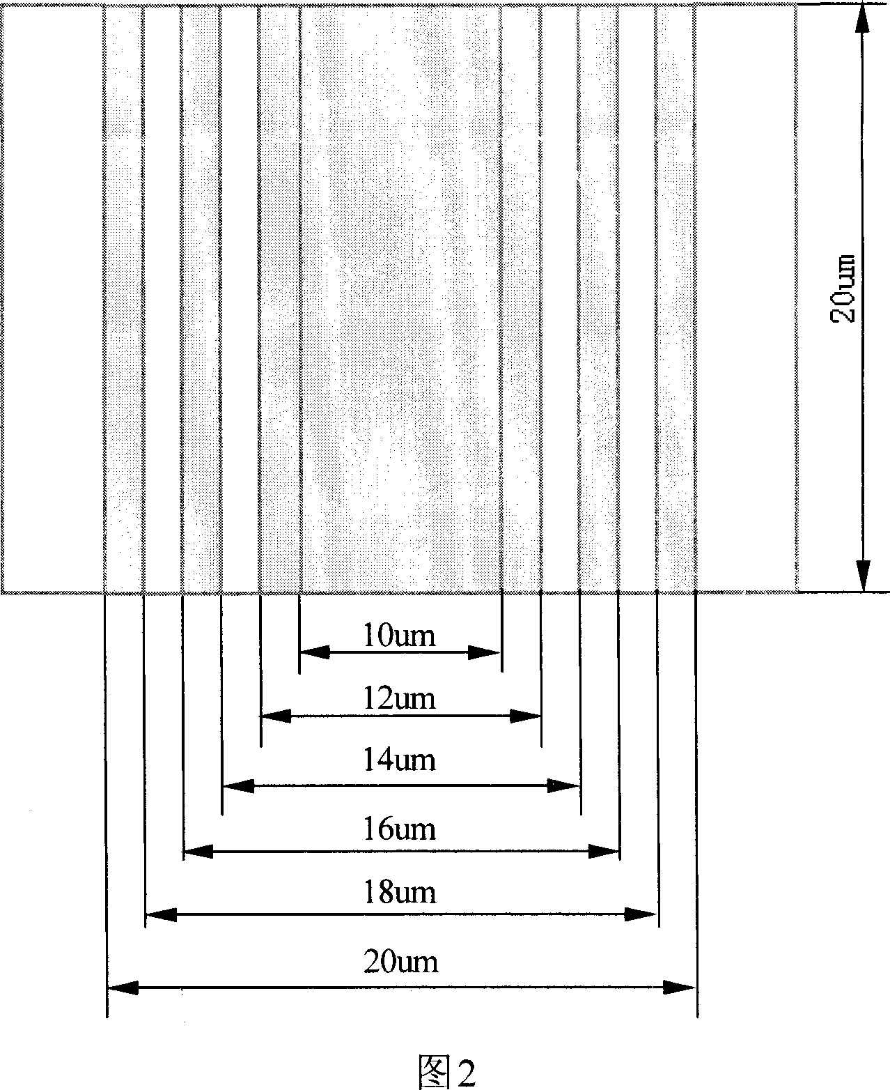
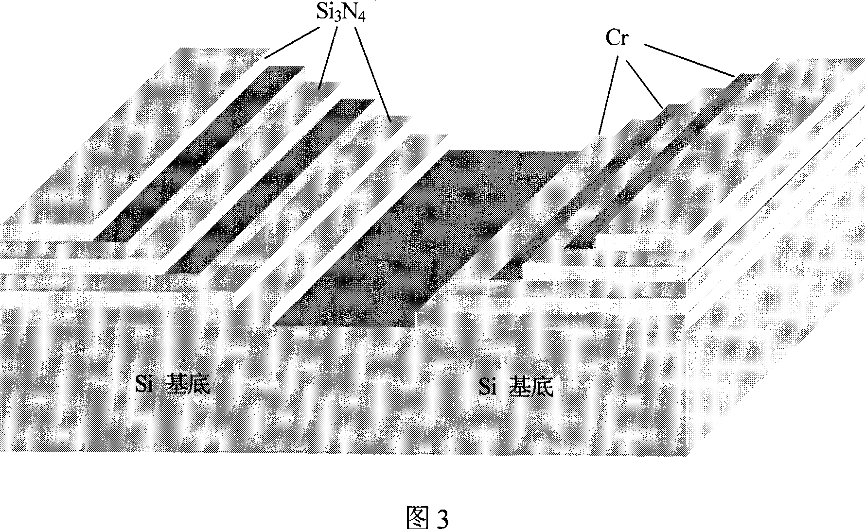
[0024] Referring to Fig. 4, the present invention comprises a base silicon wafer and alternately deposited on the base silicon wafer made of Si 3 N 4 A stepped rectangular boss composed of a thin film and a Cr thin film.
[0025] The preparation method of the present invention is as follows:
[0026] 1) Clean the silicon wafers, immerse the silicon wafers in toluene, acetone, and deionized water for 10 minutes and ultrasonically clean them for 10 minutes. After each ultrasonic washing, wash them repeatedly with a large amount of deionized water, and finally dry them with nitrogen; then put the silicon wafers into Piranha Treat in the solution at 80°C for 60 minutes, take it out, rinse it thoroughly with a large amount of deionized water, and dry it with high-purity nitrogen; the Piranha solution contains 98% sulfuric acid and 30% hydrogen peroxide with a vo...
PUM
 Abstract
Description
Claims
Application Information


