

Semiconductor memory device and manufacturing method thereof
a memory device and semiconductor technology, applied in the direction of capacitors, solid-state devices, transistors, etc., can solve the problems of deteriorating reliability, difficult to secure the required capacity, and deteriorating signal-to-noise ratio, etc., to achieve secure sufficient storage capacity, large storage capacity, and sufficient storage capacity.
- Summary
- Abstract
- Description
- Claims
- Application Information
AI Technical Summary
Benefits of technology
Problems solved by technology
Method used
Image

Examples
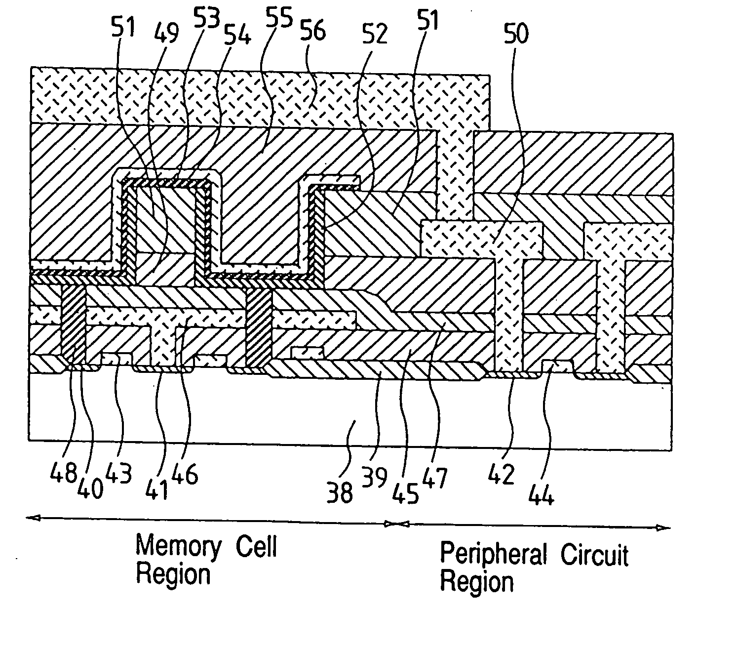
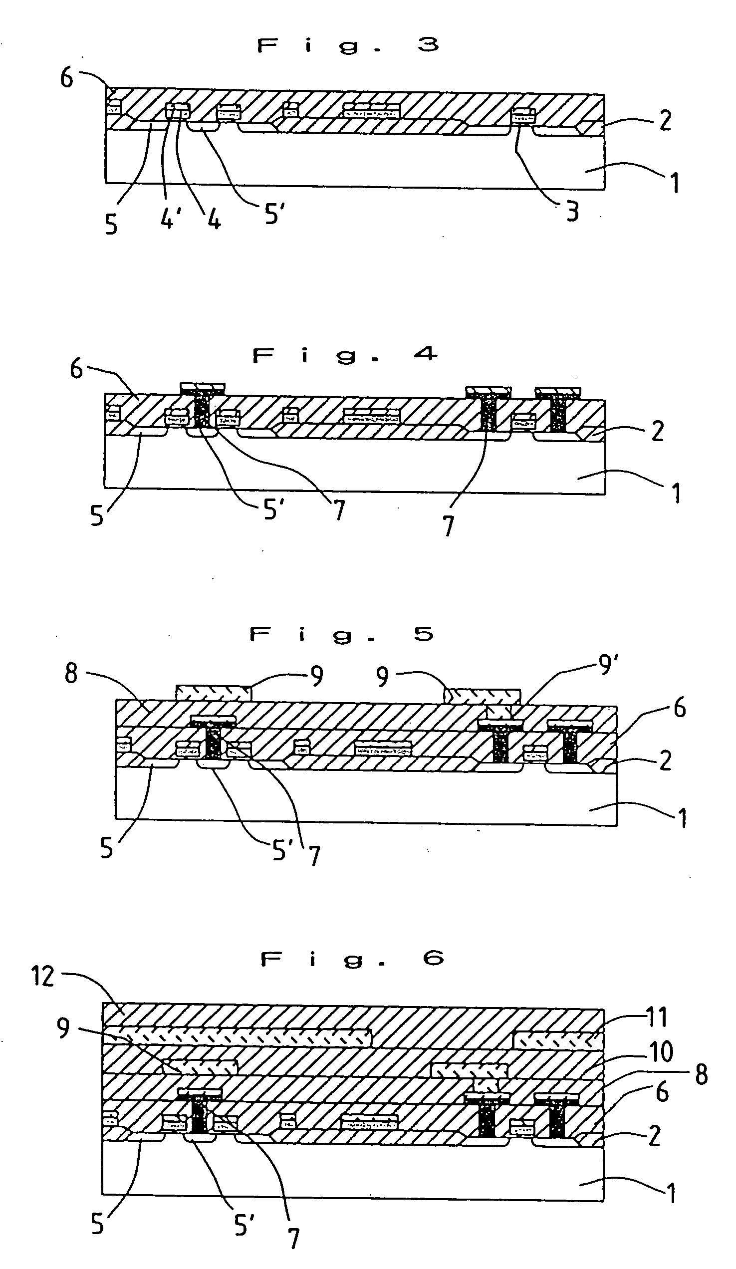
first embodiment
[0138] First, as shown in FIG. 3, an element isolating oxide film 2 for separating a MOSFET is formed on the surface of a semiconductor substrate 1 using a well-known device isolation technology.
[0139] Next, after the surface of the semiconductor substrate 1 is cleaned, a gate oxide film 3 with the thickness of 7 nm is formed at the temperature for oxidation of 800° C. by well-known thermal oxidation. A polycrystalline silicon film 4 with the thickness of 100 nm including high-density impurities is formed by well-known CVD. After a metal film 4′ with the thickness of 100 nm consisting of a stacked film constituted by a tungsten film and a barrier metal film is formed on the polycrystalline silicon film 4 so as to reduce resistance, a word line and a gate electrode 4 are formed by well-known dry etching so that they are in a predetermined shape. Arsenic approximately 5×10¹⁴ / cm2 is implanted as impurity ion with a conductive type reverse to the substrate 1 using this gate electrode 4...
second embodiment
[0164]FIG. 17 is a conceptual drawing showing a memory array equivalent to a second embodiment according to the present invention. As shown in FIG. 17, word lines WL1 to WL16 are regularly arranged vertically and bit lines BL1a, BL1b, BL2a and BL2b are connected to sense amplifiers 1 and 2 with BL1a and BL1b forming a group and BL2a and BL2b forming a group.
[0165] One bit line contact BC1 (◯) is shared by storage mode contacts CC1 and CC2 (●) connected to two memory cells.
[0166] As shown in FIG. 17, a straight line showing the active area of the MOSFET of a switching transistor between two storage mode contacts ● via the bit line contact ◯ is arranged slantwise for the word lines WL1 to WL6 and the bit lines BL1a to BL2b. In addition, the direction of the gradient is different between adjacent memory cells. Therefore, each storage mode contact CC1 and CC2 (●) can be respectively formed in clearance between the word lines WL1 to WL6 and the bit lines BL1a and BL2b.
[0167] In this e...
third embodiment
[0173] In this embodiment, as shown in FIG. 19, two storage mode contacts CC1 and CC2 in a memory cell sharing one bit line contact BC1 are arranged so that they are symmetrical on a mirror based upon each global word line W12, W34 and W56. This embodiment is different from the second embodiment in this, however, basic memory operation is similar, the layout of a global word line and a selector line which are buried wiring, which characterizes the present invention, is also similar as shown in FIG. 20 and the same effect as in the second embodiment can be obtained.
PUM
 Abstract
Description
Claims
Application Information